Heat treatment apparatus heating substrate by irradiation with light

a heat treatment apparatus and substrate technology, applied in lighting and heating apparatus, stoves or ranges, furniture, etc., can solve the problems of increasing heat capacity, no heat treatment apparatus that permits annealing time, and no conventional technique that provides annealing time within an intermediate rang

Active Publication Date: 2009-03-12
DAINIPPON SCREEN MTG CO LTD
View PDF14 Cites 46 Cited by
  • Summary
  • Abstract
  • Description
  • Claims
  • Application Information

AI Technical Summary

Benefits of technology

[0017]Providing chopper control over the light emission from the flash lamp, the heat treatment apparatus allows free setting of annealing time and the temperature profile at the time of annealing.
[0018]An object of the invention is thus to provide a heat treatment apparatus that allows free setting of annealing time and the temperature profile at the time of annealing.

Problems solved by technology

There is, however, no conventional technique that provides annealing time within an intermediate range between the range achieved by the rapid lamp annealers using halogen lamps and the range achieved by the flash lamp annealers.
In other words, there is no heat treatment apparatus that permits annealing time on the order of 10 milliseconds to 1 second at each place on the major surface of a semiconductor wafer.
The use of halogen lamps to achieve the above-described intermediate range of annealing time requires an increase in filament thickness due to the necessity of greater output and therefore has the drawback of increasing heat capacity and thereby rather slowing down the rates of temperature rise and fall.
But, keeping a pulse laser beam for a longer time at a particular place causes a temperature rise even in an unexposed region, so that the phenomenon of switching occurring in overlaps between temperature-raised regions becomes more pronounced.
An even greater drawback is impractically low throughput because about one hour is necessary to process a single semiconductor wafer as a result of an increase in the length of time that a pulse laser beam remains at each place.

Method used


Image

  • Heat treatment apparatus heating substrate by irradiation with light
  • Heat treatment apparatus heating substrate by irradiation with light
  • Heat treatment apparatus heating substrate by irradiation with light

Examples


Embodiment Construction

[0029]Now, preferred embodiments of the invention are described in detail with reference to the drawings.

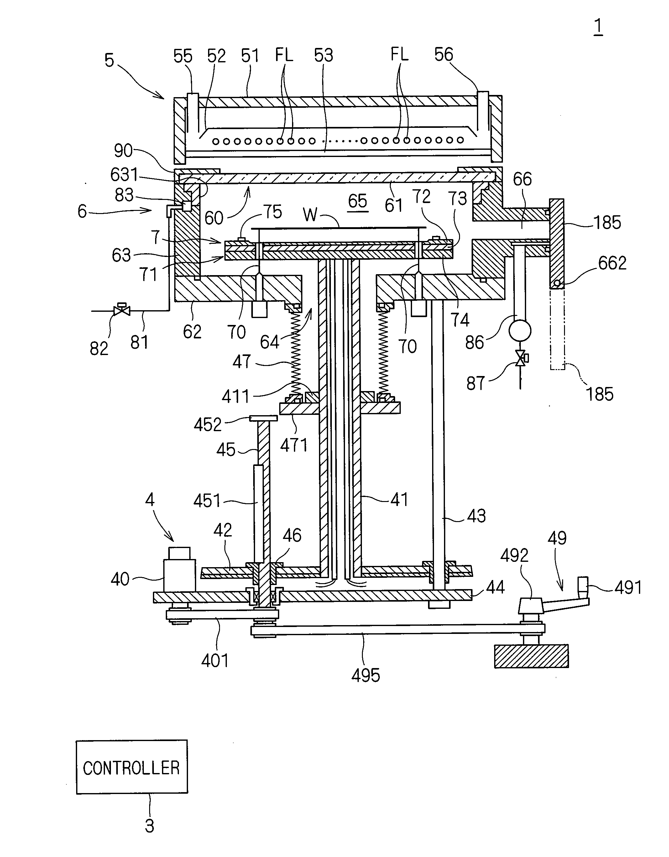
[0030]First, a general configuration of a heat treatment apparatus according to the invention is outlined. FIG. 1 is a side sectional view showing the configuration of a heat treatment apparatus 1 according to the invention. The heat treatment apparatus 1 is a lamp annealer that irradiates a generally-circular semiconductor wafer W as a substrate with light to thereby heat the semiconductor wafer W.

[0031]The heat treatment apparatus 1 includes a generally-cylindrical chamber 6 receiving a semiconductor wafer W therein, and a lamp house 5 including a plurality of built-in flash lamps FL. The heat treatment apparatus 1 further includes a controller 3 controlling and causing operating mechanisms in the chamber 6 and in the lamp house 5 to perform heat treatment on the semiconductor wafer W.

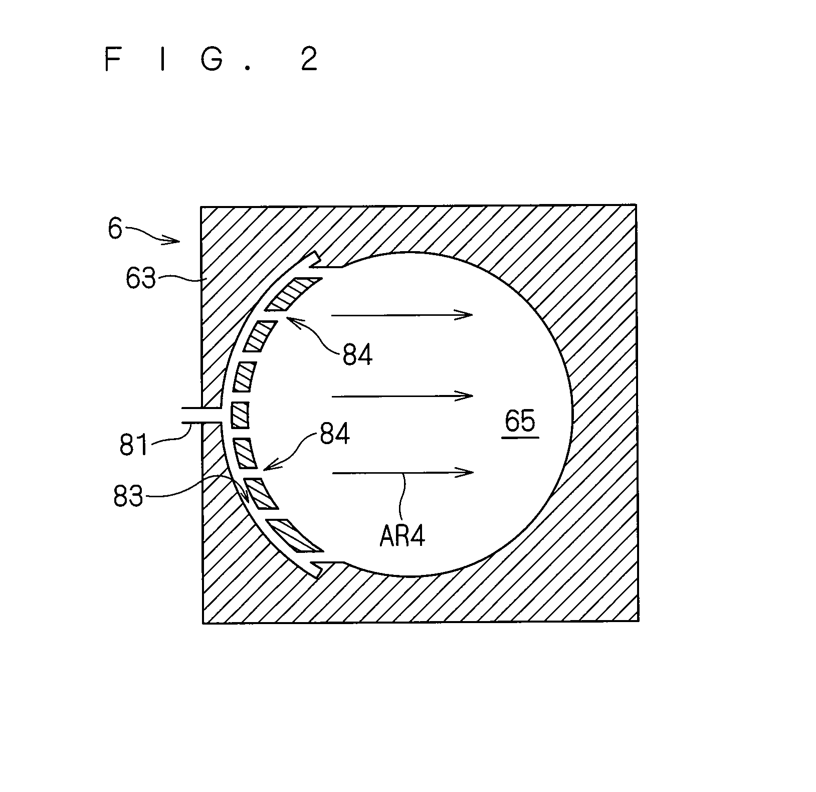
[0032]The chamber 6 below the lamp house 5 includes a chamber side portion 63 having a general...


PUM


Abstract

A capacitor, a coil, a flash lamp, and a switching element such as an IGBT are connected in series. A controller outputs a pulse signal to the gate of the switching element. A waveform setter sets the waveform of the pulse signal, based on the contents of input from an input unit. With electrical charge accumulated in the capacitor, a pulse signal is output to the gate of the switching element so that the flash lamp emits light intermittently. A change in the waveform of the pulse signal applied to the switching element will change the waveform of current flowing through the flash lamp and, accordingly, the form of light emission, thereby resulting in a change in the temperature profile for a semiconductor wafer.

Description

BACKGROUND OF THE INVENTION[0001]1. Field of the Invention[0002]The present invention relates to a heat treatment apparatus that irradiates a substrate such as a semiconductor wafer and a glass substrate for a liquid crystal display with light, to thereby heat the substrate.[0003]2. Description of the Background Art[0004]Short-time annealing has conventionally been achieved using rapid lamp annealers that use the energy of light emitted from halogen lamps to raise the temperature of a semiconductor wafer at rates of about several hundred degrees per second, as disclosed in U.S. Pat. No. 6,518,547. The rapid lamp annealers have shorter annealing time than heat treatment apparatuses that employ a resistance heating method using a kanthal heater or the like, but their annealing time is only on the order of several seconds.[0005]On the other hand, flash lamp annealers that employ xenon flash lamps to irradiate a semiconductor wafer surface with a flash of light, as disclosed in U.S. Pat...

Claims


Application Information

Patent Timeline
Patent Type & Authority Applications(United States)
IPC IPC(8): F26B3/28
CPCH01L21/67115H01L21/68742H01L21/68785H01L2924/0002H05B1/0227H01L21/26H01L2924/00H01L21/324
Inventor KUSUDA, TATSUFUMI
Owner DAINIPPON SCREEN MTG CO LTD
Why Eureka
Try Eureka