Thermo-compression bonded electrical interconnect structure and method

Inactive Publication Date: 2009-03-19
ULTRATECH INT INC
View PDF32 Cites 45 Cited by
  • Summary
  • Abstract
  • Description
  • Claims
  • Application Information

AI Technical Summary

Benefits of technology

[0051]The present invention advantageously provides a simple structu

Problems solved by technology

Connections between structures are typi

Method used


Image

  • Thermo-compression bonded electrical interconnect structure and method
  • Thermo-compression bonded electrical interconnect structure and method
  • Thermo-compression bonded electrical interconnect structure and method

Examples


Embodiment Construction

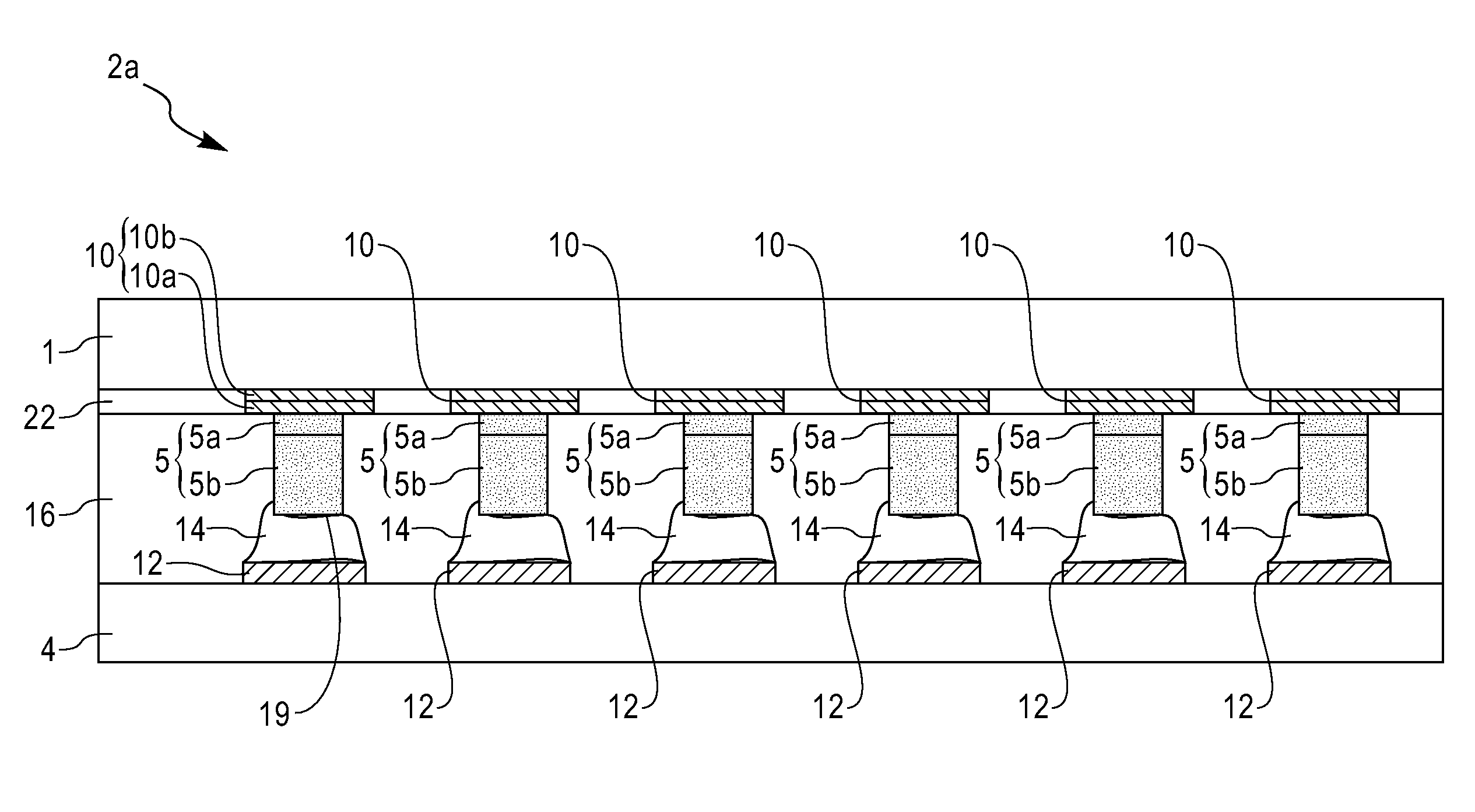
[0063]FIG. 1 illustrates a cross sectional view of an electrical structure 2a, in accordance with embodiments of the present invention. Electrical structure 2a comprises a substrate 1, a substrate 4, a plurality of interconnect structures 5, an optional layer of adhesive 22, and an optional layer(s) 16 of underfill encapsulant material. Substrate 1 comprises a plurality of electrically conductive pads 10. Each pad of electrically conductive pads 10 may be connected to wires or electrical components within substrate 1. Substrate 4 comprises a plurality of electrically conductive pads 12. Each pad of electrically conductive pads 12 may be connected to wires or electrical components within substrate 4. Substrate 1 may comprise, inter alia, a semiconductor device (e.g., an integrated circuit chip, a semiconductor wafer, etc), a chip carrier (organic or inorganic), a printed circuit board, etc. Substrate 4 may comprise, inter alia, a semiconductor device (e.g., an integrated circuit chip...


PUM

PropertyMeasurementUnit
Electrical conductivityaaaaaaaaaa
Metallic bondaaaaaaaaaa
Biodegradabilityaaaaaaaaaa

Abstract

An electrical structure and method for forming electrical interconnects. The method includes positioning a sacrificial carrier substrate such that a first surface of a non-solder metallic core structure within the sacrificial carrier substrate is in contact with a first electrically conductive pad. The first surface is thermo-compression bonded to the first electrically conductive pad. The sacrificial carrier substrate is removed from the non-solder metallic core structure. A solder structure is formed on a second electrically conductive pad. The first substrate comprising the non-solder metallic core structure is positioned such that a second surface of the non-solder metallic core structure is in contact with the solder structure. The solder structure is heated to a temperature sufficient to cause the solder structure to melt and form an electrical and mechanical connection between the second surface of the non-solder metallic core structure and the second electrically conductive pad.

Description

FIELD OF THE INVENTION[0001]The present invention relates to a thermo-compression bonded electrical interconnect structure and method for forming.BACKGROUND OF THE INVENTION[0002]Connections between structures are typically unreliable and subject to failure. Accordingly, there exists a need in the art to overcome at least one of the deficiencies and limitations described herein above.SUMMARY OF THE INVENTION[0003]The present invention provides a method for forming an electrical structure comprising:[0004]providing a first substrate comprising a first electrically conductive pad, a second substrate comprising a second electrically conductive pad, and a transfer structure, wherein said transfer structure comprises a sacrificial carrier substrate, a polymer release layer formed over and in contact with said sacrificial carrier substrate, and a non-solder metallic core structure formed over and in contact with said polymer release layer, and wherein said non-solder metallic core structu...

Claims


Application Information

Patent Timeline
IPC IPC(8): H01L21/44
CPCH01L2224/81801H01L21/6835H01L2224/16H05K3/328H05K2201/10734H01L24/12H05K3/3436H05K2201/0379H05K2201/0367H01L2224/13147H01L2924/01022H01L2924/01023H01L2224/13611H01L2924/14H01L2224/13655H01L2224/1357H01L2924/00013H01L24/11H01L2924/01024H01L2224/81193H01L2924/01079H05K2203/0338H01L24/81H01L2224/81191H01L2224/11901H05K2201/10234H01L2924/01029H01L2224/13644H01L2924/01006H01L2224/11003H01L21/563H01L2224/13144H05K2201/10977H01L2924/01078H01L2224/81203H01L2224/13082H01L24/16H01L2924/014H01L2924/01033H01L2224/73203Y10T29/49155H01L2224/11334H01L2924/0105H01L2924/00014H01L2224/13099H01L24/05H01L2224/05001H01L2224/05026H01L2224/0508H01L2224/05144H01L2224/05147H01L2224/05155H01L2224/05166H01L2224/05171H01L2224/05571H01L2224/05644Y02P70/50
Inventor FURMAN, BRUCE K.NAH, JAE-WOONG
Owner ULTRATECH INT INC
Why Eureka
Try Eureka