Techniques for optical ion beam metrology

a technology of optical ion beam and metrology, applied in the direction of beam deviation/focusing by electric/magnetic means, instruments, etc., can solve the problems of ribbon beams that cannot be uniformly beamlets may not be evenly spaced within the ribbon beam, and ribbon beams that lack angle uniformity and/or dose uniformity, etc., to achieve the effect of enhancing the image of the ion beam

Inactive Publication Date: 2009-03-26
VARIAN SEMICON EQUIP ASSOC INC
View PDF15 Cites 8 Cited by
  • Summary
  • Abstract
  • Description
  • Claims
  • Application Information

AI Technical Summary

Benefits of technology

[0020]In accordance with other aspects of this particular exemplary embodiment, the

Problems solved by technology

However, just like spot beams, ribbon beams can suffer from intrinsic non-uniformity problems.
Furthermore, beamlets may not be evenly spaced within the ribbon beam.
Therefore, a ribbon beam may lack angle uniformity and/or dose uniformity.
Although these additional components have been utilized in conventional ion implanters to improve either angle uniformity or dose uniformity of a ribbon beam, a more efficient solution has yet to be made available for providing ribbon

Method used


Image

  • Techniques for optical ion beam metrology
  • Techniques for optical ion beam metrology
  • Techniques for optical ion beam metrology

Examples


Embodiment Construction

[0031]Embodiments of the present disclosure provide an ion implantation solution that improves measurement of ion beam profiles and ion beam angles using optical ion beam metrology.

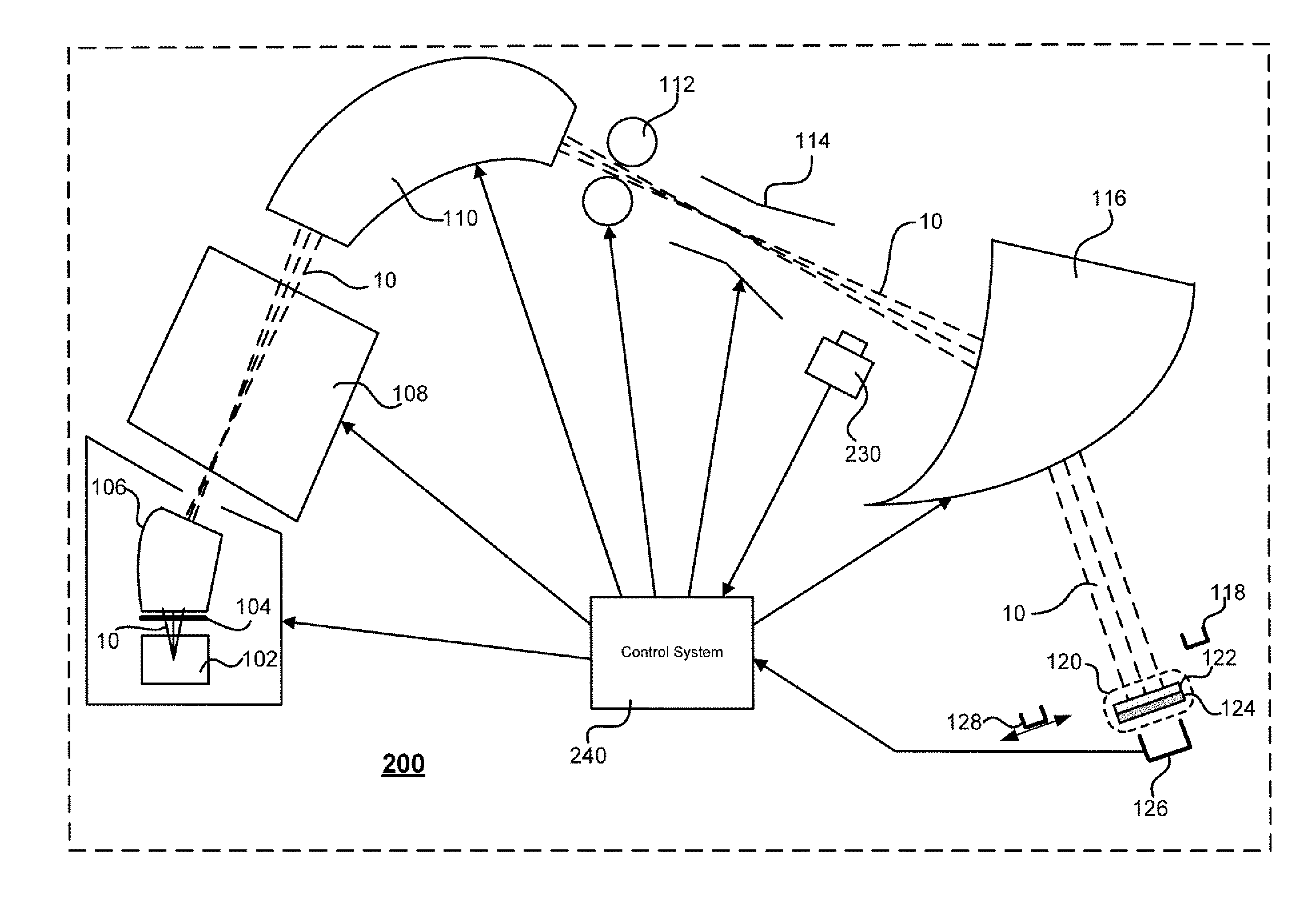
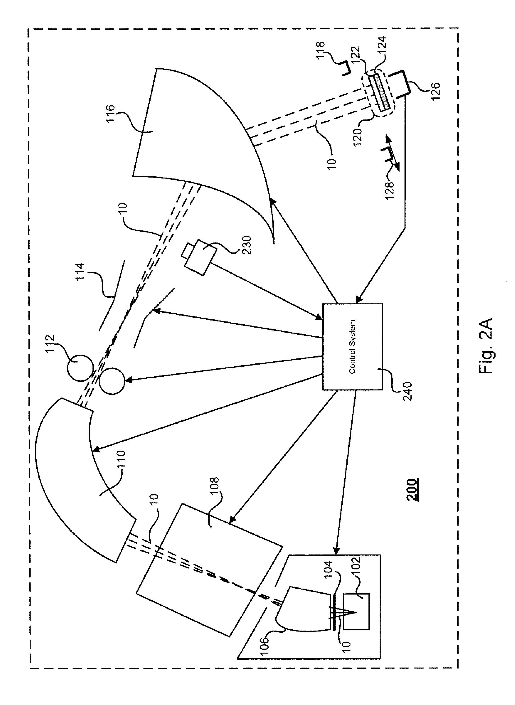
[0032]Referring to FIG. 2A, there is shown an exemplary ion implanter system configuration 200 in accordance with an embodiment of the present disclosure. The ion implanter system 200 of FIG. 2A incorporates all of the elements of FIG. 1. In addition, the ion implanter system 200 may include a camera 230 and a control system 240. The camera 230 may be positioned adjacent to an ion beam 10 for taking one or more images of the ion beam 10. The ion beam 10 may be viewed through the camera 230 via at least one window on the chamber. In one embodiment, the one or more images of the ion beam 10 may be stored in the camera 230. In another embodiment, the one or more images of the ion beam 10 may be transmitted to the control system 240 for storage in one or more storage mediums (e.g., database) (not shown) at th...


PUM


Abstract

Techniques for providing optical ion beam metrology are disclosed. In one particular exemplary embodiment, the techniques may be realized as an apparatus for controlling beam density profile, the apparatus may include one or more camera systems to capture at least one image of an ion beam and a control system coupled to the one or more camera systems to control a beam density profile of the ion beam. The control system may further include a dose profiler to provide information to one or more ion implantation components in at least one of a feedback loop and a feedforward loop to improve dose and angle uniformity.

Description

FIELD OF THE DISCLOSURE[0001]The present disclosure relates generally to semiconductor manufacturing equipment and, more particularly, to techniques for optical ion beam metrology.BACKGROUND OF THE DISCLOSURE[0002]Ion implantation is a process of depositing chemical species into a substrate by direct bombardment of the substrate with energized ions. In semiconductor manufacturing, ion implanters are used primarily for doping processes that alter the type and level of conductivity of target materials. A precise doping profile in an integrated circuit (IC) substrate and its thin-film structure is often crucial for proper IC performance. To achieve a desired doping profile, one or more ion species may be implanted in different doses and at different energy levels.[0003]In an ion implantation process, an ion beam typically scans a wafer or substrate surface. As used hereinafter, “scanning” a wafer or substrate surface with an ion beam refers to the relative movement of the ion beam with...

Claims


Application Information

Patent Timeline
IPC IPC(8): G21K1/00
CPCH01J37/244H01J37/304H01J37/3171H01J2237/30472H01J2237/24507H01J2237/24542H01J2237/2482H01J2237/2445
Inventor PEREL, ALEXANDER S.PLATOW, WILHELMCHANEY, CRAIGSINCLAIR, FRANKROCKWELL, TYLER
Owner VARIAN SEMICON EQUIP ASSOC INC
Why Eureka
Try Eureka