
Semiconductor substrate elastomeric stack

Active Publication Date: 2009-03-26
MICROSS ADVANCED INTERCONNECT TECH LLC
View PDF38 Cites 9 Cited by
  • Summary
  • Abstract
  • Description
  • Claims
  • Application Information

AI Technical Summary

Benefits of technology

[0011]In one advantageous aspect, long (>two inches) metal conductors on the semiconductor substrates do not break even though the metal of the long conductors expands and contracts with temperature differently than the supporting semiconductor

Problems solved by technology

Unfortunately, the communication bandwidth between the flying UAV and the control base on the ground where the analysis is to be performed is often inadequate to stream all the gathered information back to the control base for analysis.
Due to the delay in this process, the object may have moved and may no longer be available for surveillance by the time the UAV returns.
The delay and cost associated with having to analyze the gathered information on the ground is undesirable.
Not only would such a conventional system be unrealistically large and heavy to place in the UAV, but the system would consume over fifteen thousand watts of electrical energy.
Providing the regulated DC power necessary to provide this very large amount electrical energy would add tremendous additional weight and size to the system.

Method used


Image

  • Semiconductor substrate elastomeric stack
  • Semiconductor substrate elastomeric stack
  • Semiconductor substrate elastomeric stack

Examples


Embodiment Construction

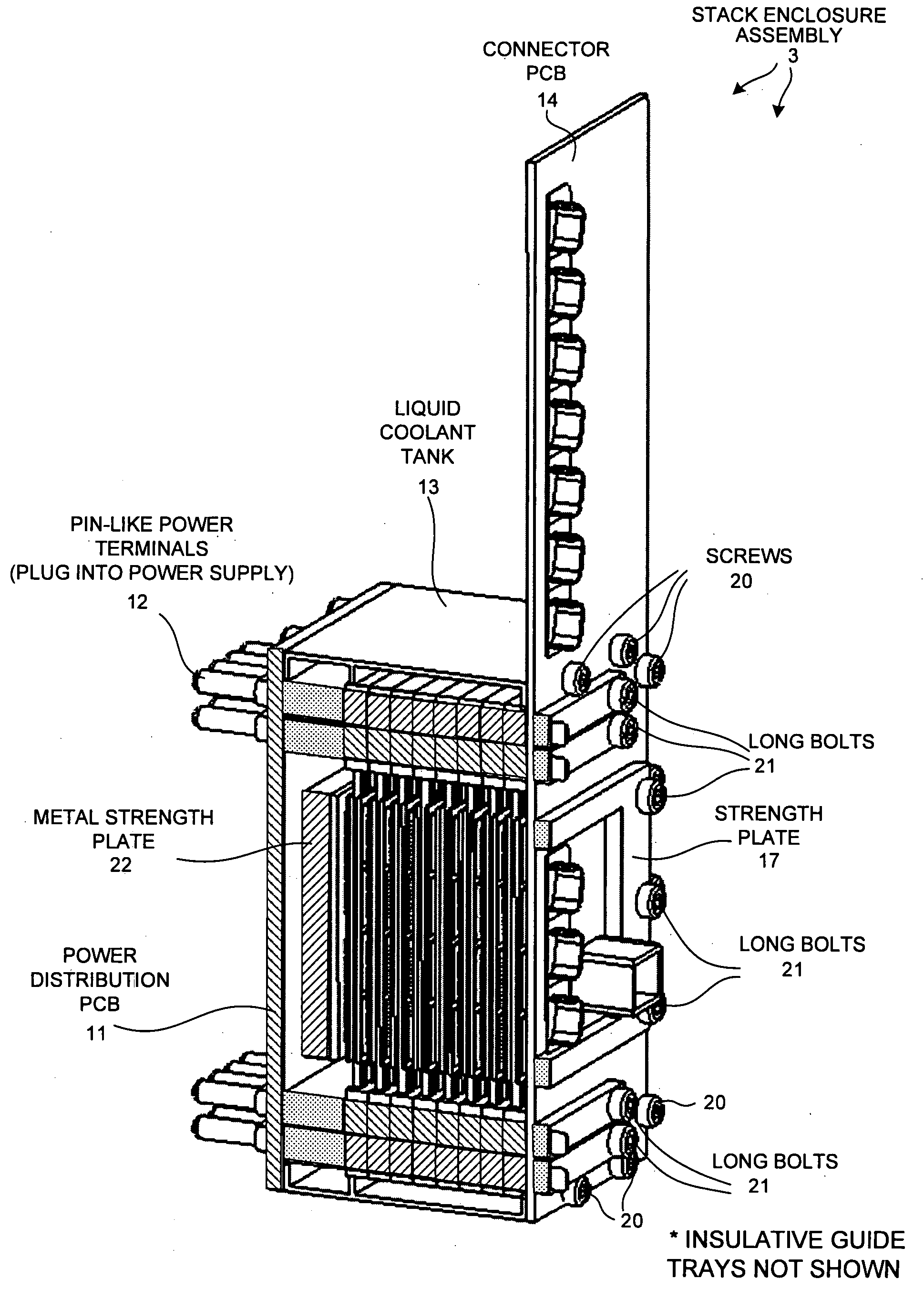
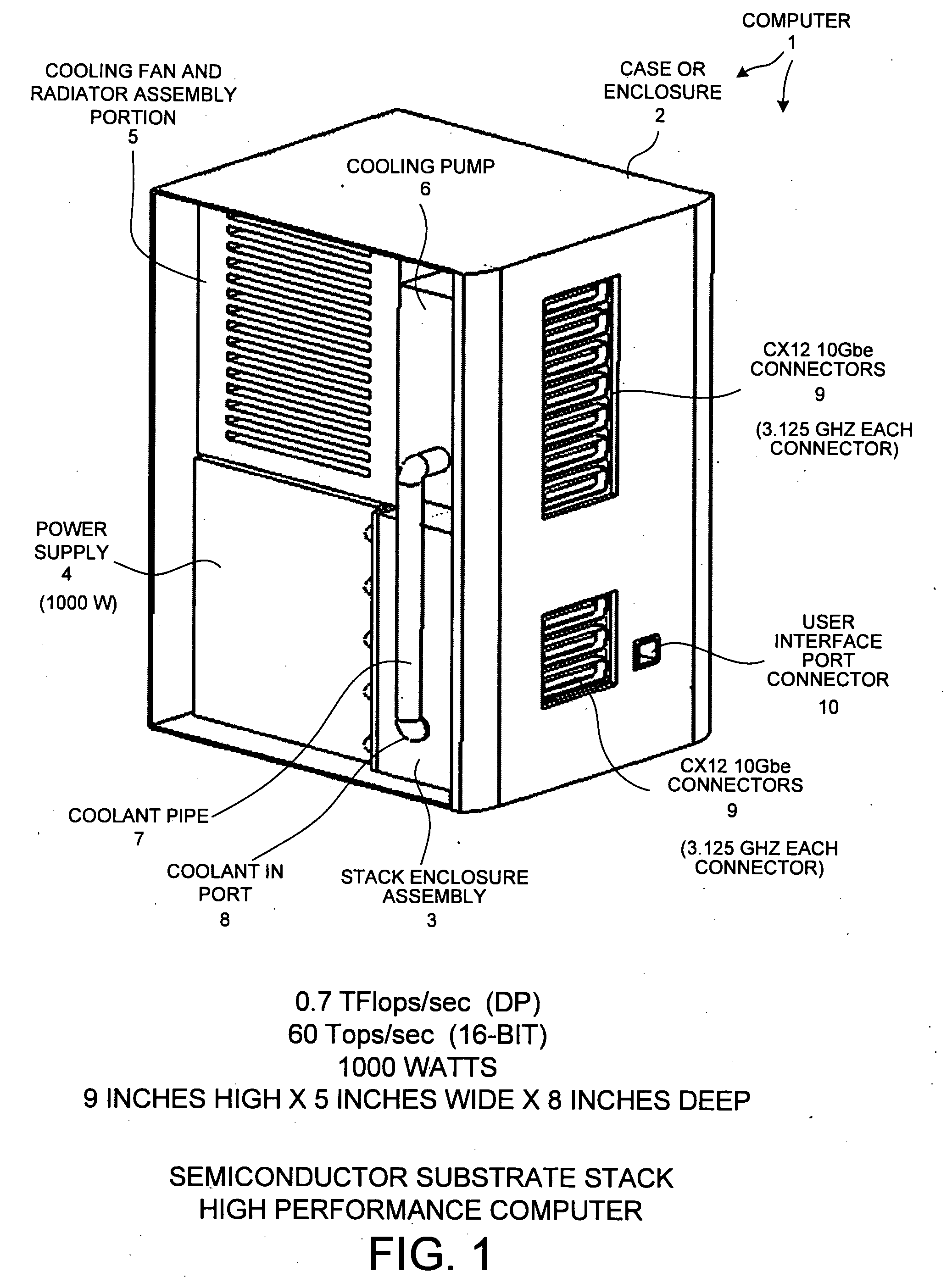
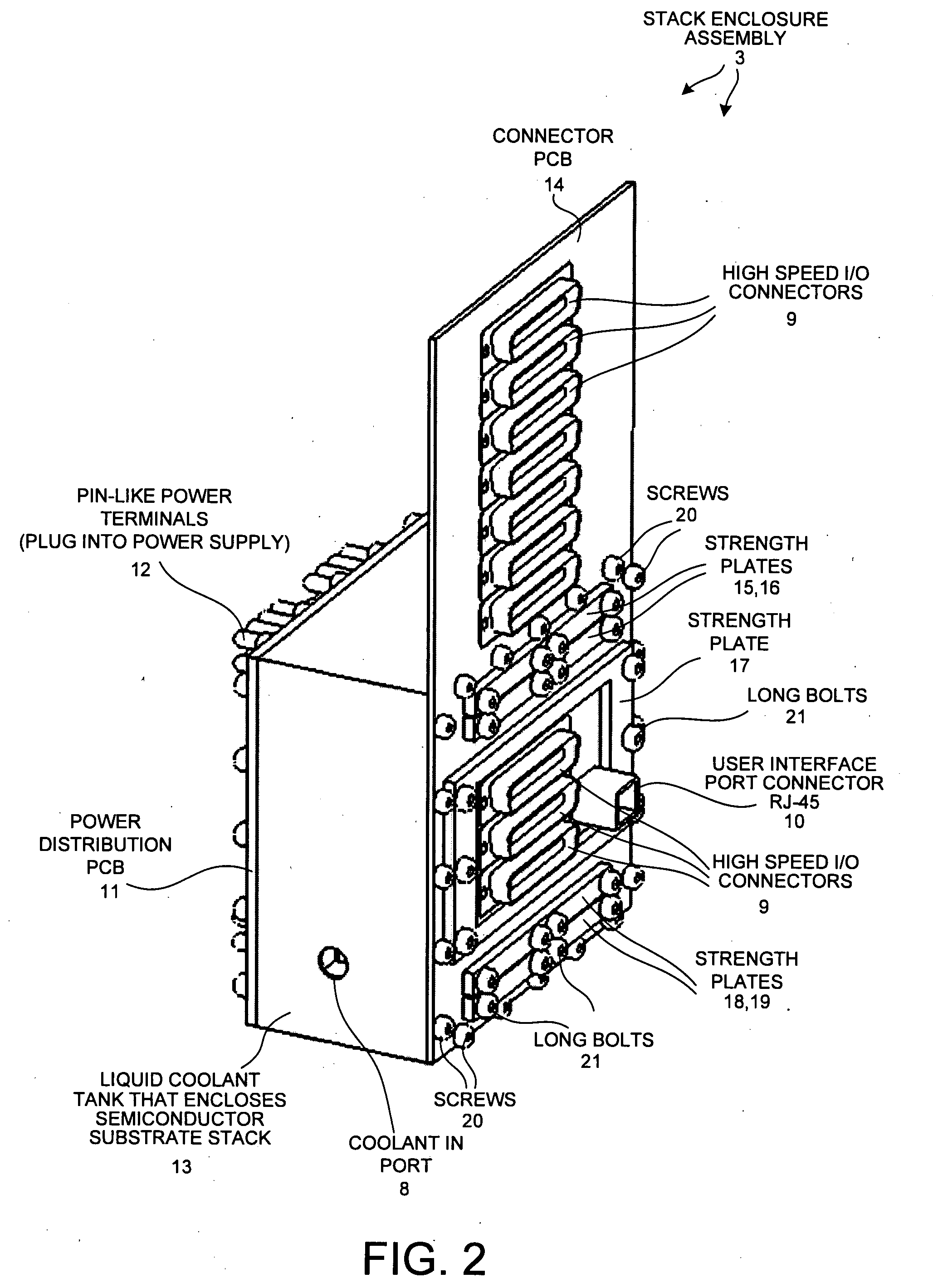
[0057]FIG. 1 is a perspective view of a novel semiconductor substrate stack high performance computer 1. Computer 1 has an approximate compute power density of 0.7 teraflops per second (10E12 double precision floating point operations per second) in a volume of less than three-hundred sixty cubic inches, and consumes less than 1000 watts. Computer 1 includes a case or enclosure 2. Case 2 retains a stack enclosure assembly 3, a power supply 4, a cooling fan and radiator assembly portion 5, a cooling pump 6, and an associated coolant pipe 7. Cooling pump 6 circulates liquid coolant, such as a fluorocarbon liquid coolant, from pump 6, through pipe 7, into coolant in port 8, through the stack enclosure assembly 3 to pick up heat, and then through the fan and radiator assembly portion 5 so that heat generated in the stack enclosure assembly 3 can be exhausted from the computer. The coolant liquid is returned from radiator assembly portion 5 to coolant pump 6 for recirculation. With appro...


PUM


Abstract

A reconfigurable high performance computer occupies less than 360 cubic inches and has an approximate compute power of 0.7 teraflops per second while consuming less than 1000 watts. The computer includes a novel stack of semiconductor substrate assemblies. Some semiconductor substrate assemblies involve field programmable gate array (FPGA) dice that are directly surface mounted, as bare die, to a semiconductor substrate. Other semiconductor substrate assemblies of the stack involve bare memory integrated circuit dice that are directly surface mounted to a semiconductor substrate. Elastomeric connectors interconnect adjacent semiconductor substrates proceeding down the stack. Tines of novel comb-shaped power bus bar assembly structures extend into the stack to supply DC supply voltages. The supply voltages are supplied from bus bars, through vias in the semiconductor substrates, and to the integrated circuits on the other side of the substrates. The power bus bars also serve as capacitors and guides for liquid coolant.

Description

CROSS REFERENCE TO RELATED APPLICATION[0001]This application claims the benefit under 35 U.S.C. §119 from provisional U.S. patent application Ser. No. 60 / 995194, entitled “Semiconductor Substrate Stack High Performance Computer,” by Robert O. Conn, filed on Sep. 24, 2007, the subject matter of which is incorporated herein by reference.TECHNICAL FIELD[0002]The described embodiments relate to high performance computing, and more particularly to reconfigurable high performance computing.BACKGROUND INFORMATION[0003]There are many uses for computers having very high computational powers. Uses include simulating how large physical systems act and interact, performing circuit simulation of very large integrated circuits, wind tunnel simulation, 3-dimensional modeling, solving stream matching problems and nearest neighbor problems, DNA and protein sequencing, and solving many other problems in industry and the sciences.[0004]Not only are there many needs for computers having high computatio...

Claims


Application Information

Patent Timeline
IPC IPC(8): H01L23/538H01L21/58
CPCH01L23/473H01L23/481H01L24/05H01L24/29H01L24/32H01L25/0652H01L2224/0557H01L2224/29101H01L2225/0652H01L2225/06527H01L2225/06541H01L2225/06555H01L2225/06572H01L2225/06589H01L2924/0002H01L2924/01005H01L2924/01006H01L2924/01013H01L2924/01019H01L2924/01029H01L2924/01033H01L2924/01074H01L2924/01077H01L2924/014H01L2924/14H01L2924/19041H01L2924/19042H05K7/20927H01L2924/00H01L2224/05552
Inventor CONN, ROBERT O.
Owner MICROSS ADVANCED INTERCONNECT TECH LLC
Learn More