Temperature Dependent Bias for Minimal Stand-by Power in CMOS Circuits

Inactive Publication Date: 2009-03-26
IBM CORP
View PDF17 Cites 12 Cited by
  • Summary
  • Abstract
  • Description
  • Claims
  • Application Information

AI Technical Summary

Benefits of technology

[0004]Embodiments of the present invention further disclose a method for reducing a temperature dependent leakage current in a semiconductor circuit. The method includes the sensing of the temperature dependent leakage current of at least one monitor FET. The method further includes the generation of a bias voltage in proportion to the sensed temperature

Problems solved by technology

As FET (Field-Effect-Transistor) devices are being scaled down, the technology becomes more complex, and device behavior deviates from the ideal textbook case.
One problem is leakage current in off-state FET devices.
Although such leakage current my be small, with the large number of devices, in excess of 107 in some semiconductor circuits, and with the leakage current continuously flowing, the power consumption due to leakage current in the stand-by mode of the circuits is a significant proble

Method used


Image

  • Temperature Dependent Bias for Minimal Stand-by Power in CMOS Circuits
  • Temperature Dependent Bias for Minimal Stand-by Power in CMOS Circuits
  • Temperature Dependent Bias for Minimal Stand-by Power in CMOS Circuits

Examples


Embodiment Construction

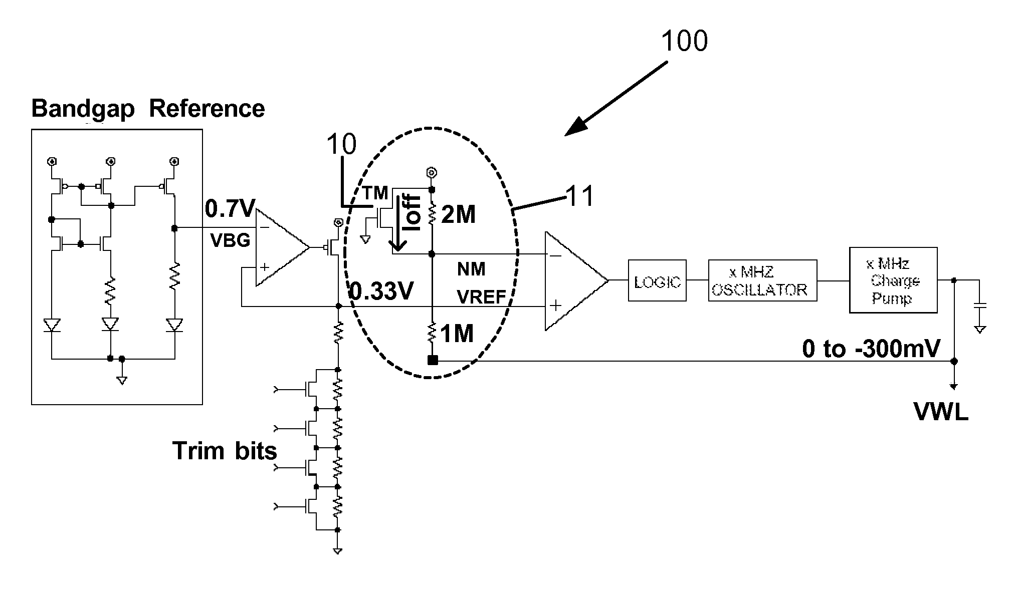
[0017]It is understood that Field Effect Transistor (FET) devices are well known in the electronic arts. Standard contacts to the FET, include the source electrode, the drain electrode, the gate electrode, and the body terminal. Terminal and electrode are equivalent terms used in the art. There are two type of FET devices: a hole conduction type, called PFET, and an electron conduction type, called NFET. Often, but not exclusively, PFET and NFET devices on the same chip are wired into CMOS circuits. A CMOS circuit contains at least one PFET device and at least one NFET device.

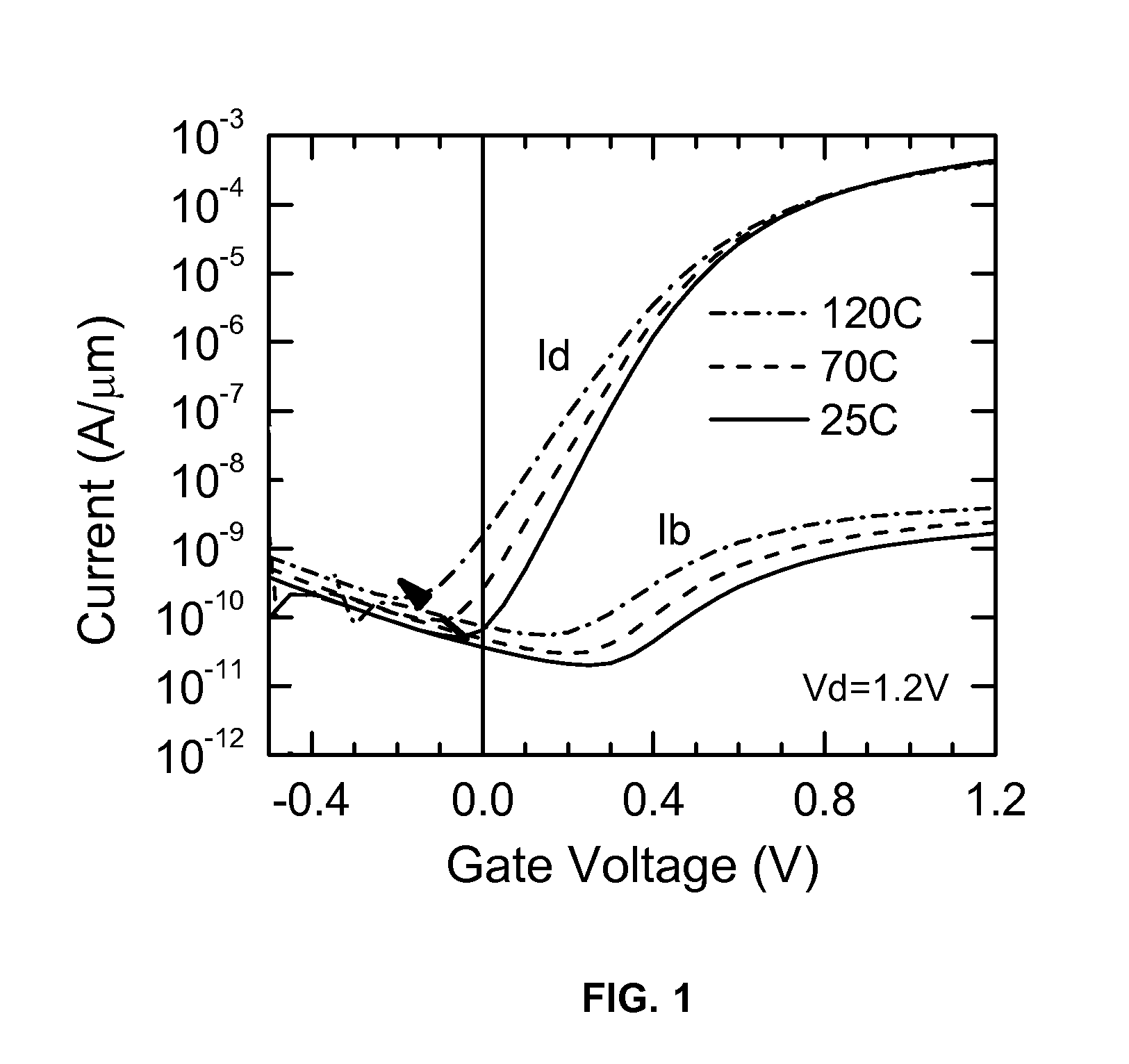
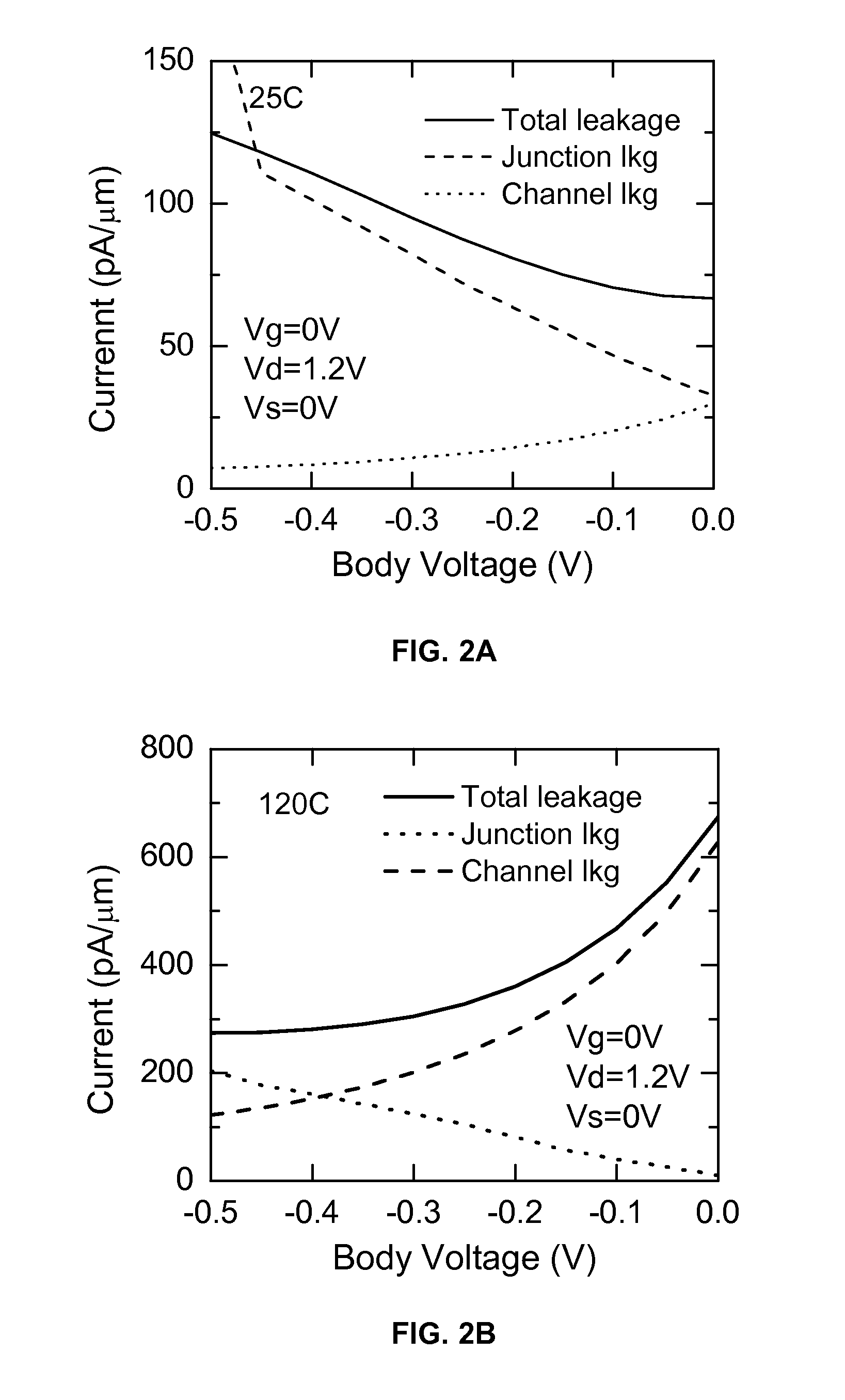
[0018]In FET operation an inherent electrical attribute is the threshold voltage. When the voltage between the source and the gate exceeds the threshold voltage, in the so called on-state, the FETs are capable to carry current between the source and the drain. When the voltage between the source and the gate is less than the threshold voltage, in the so called off-state, the FETs are not carrying current betwee...


PUM


Abstract

A circuit is disclosed which generates such a bias voltage that when this bias voltage is received by a large plurality of devices of a semiconductor chip, power consumption is reduced in the stand-by mode at any particular operating temperature. The disclosed circuit contains at least one monitor FET, which is kept in its off-state, and which has common properties with the large plurality of FET devices. The temperature dependent leakage current of the monitor FET is sensed, and used to generate the bias voltage in proportion to the leakage current. This bias voltage is received by the large plurality FET devices on their gate electrodes, or on their body terminals.

Description

FIELD OF THE INVENTION[0001]The present invention is related to semiconductor integrated circuits, and more particularly to a system and method for minimizing power consumption in the stand-by mode at all operating temperatures.BACKGROUND OF THE INVENTION[0002]Today's integrated circuits include a vast number of devices. As FET (Field-Effect-Transistor) devices are being scaled down, the technology becomes more complex, and device behavior deviates from the ideal textbook case. One problem is leakage current in off-state FET devices. Although such leakage current my be small, with the large number of devices, in excess of 107 in some semiconductor circuits, and with the leakage current continuously flowing, the power consumption due to leakage current in the stand-by mode of the circuits is a significant problem. As devices are becoming ever smaller, the stand-by mode power consumption problem is expected to increase. There are fabrication and device design techniques which aim to d...

Claims


Application Information

Patent Timeline
IPC IPC(8): G05F1/567G11C7/04H03K17/16
CPCH03K19/00369H03K19/0016
Inventor CAI, JINMANN, RANDY WILLIAMPILO, HAROLD
Owner IBM CORP
Why Eureka
Try Eureka