Air gap structure design for advanced integrated circuit technology

a technology of integrated circuits and air gaps, applied in the direction of semiconductor devices, basic electric elements, electrical equipment, etc., can solve the problems of elk also having a high cost, cracking and/or delamination of ild materials, increasing cost and cycle time,

Inactive Publication Date: 2009-03-26
TAIWAN SEMICON MFG CO LTD
View PDF14 Cites 38 Cited by
  • Summary
  • Abstract
  • Description
  • Claims
  • Application Information

AI Technical Summary

Problems solved by technology

There are many reliability issues when using ELK dielectrics, in particular packaging problems.
When ELK and ultra low-k (ELK) materials are used, the thermal mismatch between the die and the package substrate can cause cracking and / or delamination of the ILD material.
ELK also has a high cost.
Integration of ELK requires a very complicated process flow (e.g. pore sealing, UV / e-beam cure, and the like), which increases cost and cycle time.
ELK has a low thermal conductivity (<0.2 W / m-C), which impedes thermal dissipation and causes electromigration and other thermal related reliability problems.

Method used


Image

  • Air gap structure design for advanced integrated circuit technology
  • Air gap structure design for advanced integrated circuit technology
  • Air gap structure design for advanced integrated circuit technology

Examples


Embodiment Construction

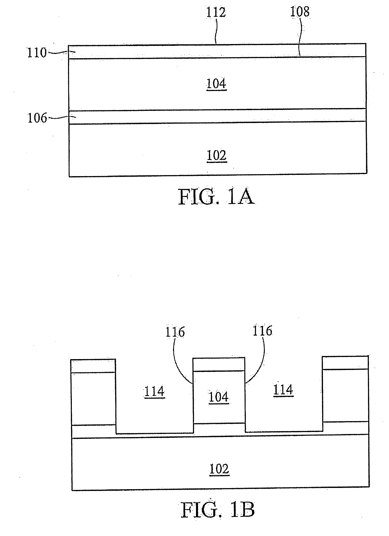
[0013]FIG. 1A shows substrate 102 and material layer 104 formed thereover. Layer 106 is interposed therebetween and may be an etch stop layer in one exemplary embodiment. Layer 106 may represent any of various other films used in semiconductor device fabrication, in other exemplary embodiments. Top layer 110 is formed over upper surface 108 of material layer 104. Top layer 110 includes upper surface 112 and may be an anti-reflective coating, ARC, or top layer 110 may be SiON or SiC or other suitable material with CH3 functional groups. Material layer 104 may be a dielectric film and material layer 104 may advantageously be a low-k, k=2.9-2.5, dielectric film. Substrate 102 may be any of various suitable substrates used in the semiconductor manufacturing industry such as silicon.

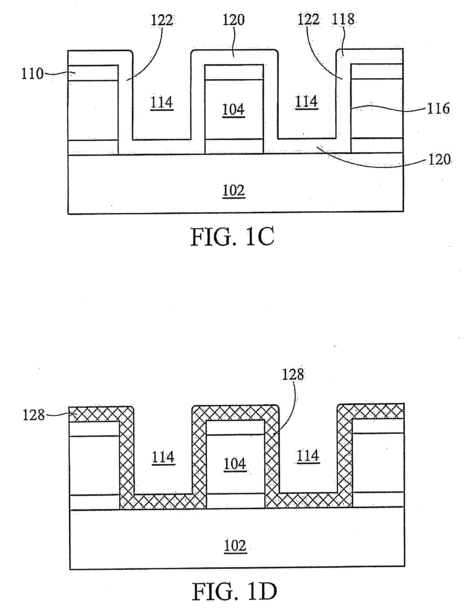
[0014]Conventional means are then used to form openings 114 shown in FIG. 1B. Openings 114 extend through top layer 110, material layer 104 and layer 106 and are bounded by sidewalls 116. In one exemplary emb...


PUM

PropertyMeasurementUnit
thicknessesaaaaaaaaaa
widthaaaaaaaaaa
dielectric constantaaaaaaaaaa

Abstract

A method for forming air gaps between interconnect structures in semiconductor devices provides a sacrificial layer formed over a dielectric and within openings formed therein. The sacrificial layer is a blanket layer that is converted to a material that is consumable in an etchant composition that the dielectric material and a subsequently formed interconnect material are resistant to. After the interconnect material is deposited a planarized surface including portions of the dielectric material, vertical sections of the converted material and portions of the interconnect material is produced. The etchant composition then removes the converted material thereby forming voids. A capping layer is formed over the structure resulting in air gaps. A sidewall protection layer may be optionally formed between the interconnect structure and the sacrificial material. In some embodiments an ARC layer may be formed over the dielectric and form part of the planar surface.

Description

FIELD OF THE INVENTION[0001]The present invention is related most generally to semiconductor device fabrication, and more specifically to interconnect structures and reducing capacitance between interconnect lines.BACKGROUND[0002]As, the semiconductor industry migrates to 90 nanometer and smaller technologies, the minimum distance between adjacent inner connect lines grows smaller. Inter-level dielectric materials (ILD) such as silicon oxide are being replaced by low-k dielectric materials, to reduce the capacitance between nearby interconnect lines. At the 32 and 45 nanometer nodes, the capacitance problem is even more acute. Typical methods to reduce capacitance between interconnect lines include using an ILD (Inter-Layer-Dielectric) or IMD (Inter Metal Dielectric) material with a lower k value, such as FSG, carbon-doped silicon oxide (e.g., BLACK DIAMOND® produced by the Applied Materials Company) and extreme low-k (ELK) dielectrics having a k value less than 2.5, to reduce inter...

Claims


Application Information

Patent Timeline
Patent Type & Authority Applications(United States)
IPC IPC(8): H01L21/4763
CPCH01L21/76831H01L21/7682H01L2221/1063
Inventor CHEN, HSIEN-WEITSAI, HAO-YIJENG, SHIN-PUULIU, BENSON
Owner TAIWAN SEMICON MFG CO LTD
Why Eureka
Try Eureka