Semiconductor device and manufacturing method thereof

Inactive Publication Date: 2009-04-02
RENESAS ELECTRONICS CORP
View PDF6 Cites 17 Cited by
  • Summary
  • Abstract
  • Description
  • Claims
  • Application Information

AI Technical Summary

Benefits of technology

[0017]According to the above-described method of manufacturing a semiconductor device of the present invention, there may be stably obtained a low layer resistance, because a metal cap film having Co as a main component is selectively grown on a metallic silicide layer having Ni as a main component on a diffusion layer, and, the metallic silicide layer having Ni as a main component is electrically connected through the metal cap film selectively provided in the upper

Problems solved by technology

However, we have now discovered that in addition to a proble

Method used


Image

  • Semiconductor device and manufacturing method thereof
  • Semiconductor device and manufacturing method thereof
  • Semiconductor device and manufacturing method thereof

Examples


first exemplary embodiment

[0040]A first exemplary embodiment according to the present invention will be explained, referring to drawings.

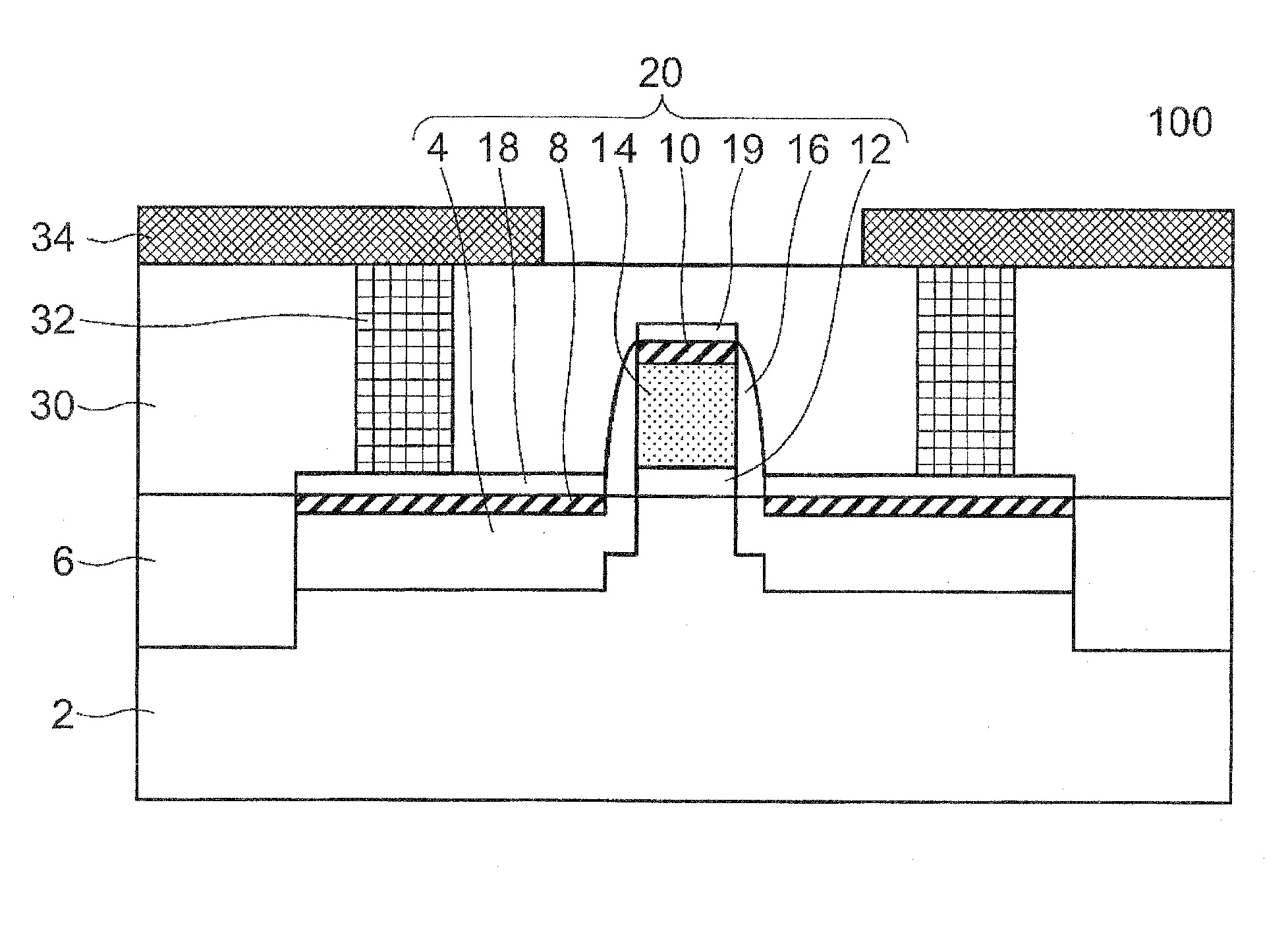
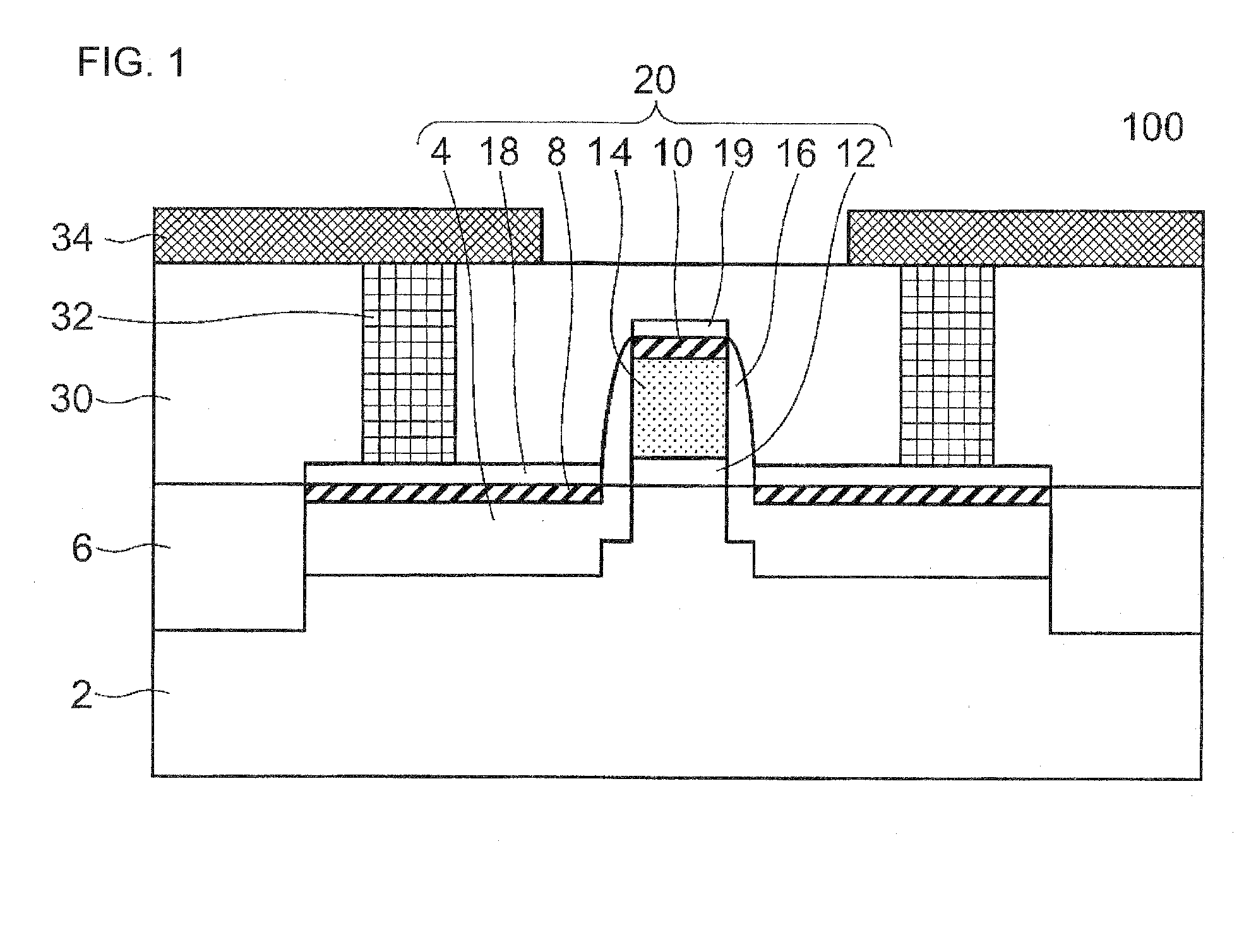
[0041]FIG. 1 is a view showing the first exemplary embodiment according to the present invention. In FIG. 1, a semiconductor device 100 has an N-channel transistor (transistor) 20 and an element isolation insulation film 6, which are formed on a P-type silicon substrate (semiconductor substrate) 2. The N-channel transistor 20 has: an N-type diffusion layer 4 (diffusion layer); a Ni silicide layer (metallic silicide layer) 8 provided on the N-type diffusion layer 4; a gate insulation film 12; a gate electrode 14; a Ni silicide layer 10 formed on the gate electrode 14; and a side-wall insulation film 16 provided on the side wall of the gate electrode 4. The gate electrode 14 is formed in, for example, polysilicon.

[0042]A Ni silicide layer 8 is continuously provided on the N-type diffusion layer 204, and, selectively, a cap metal film 18 (for example, CoWP) is formed on the Ni...

second exemplary embodiment

[0059]Then, a second exemplary embodiment according to the present invention will be explained, referring to drawings.

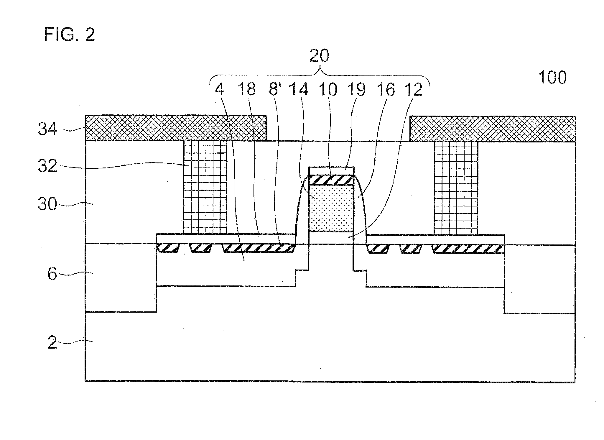
[0060]FIG. 7 is a view showing the second exemplary embodiment of the present invention. It is different from the configuration of the first exemplary embodiment that a gate electrode 15 of an N-channel transistor 20 in a semiconductor device 101 is formed with metal, as shown in FIG. 7 in the present exemplary embodiment. Furthermore, as a cap insulation film 17 is provided on the metal gate electrode 15 in the present exemplary embodiment, neither the Ni silicide layer nor the metal cap film are formed on the metal gate electrode 15, different from the configuration of the first exemplary embodiment. The cap insulation film 17 includes, for example, a silicon nitride film. Here, even in the present exemplary embodiment, the Ni silicide layer may include Pt.

[0061]Then, the method of manufacturing the present exemplary embodiment will be explained.

[0062]The method of...

third exemplary embodiment

[0065]Then, a third exemplary embodiment according to the present invention will be explained, referring to drawings.

[0066]FIG. 9 is a view showing the third exemplary embodiment according to the present invention. In this exemplary embodiment, the present invention is applied to CMOS. Hereinafter, different points between the present exemplary embodiment and the first exemplary embodiment will be mainly described, and the same points as those in the first exemplary embodiment will not be repeated.

[0067]As shown in FIG. 9, a semiconductor device 102 has the N-channel transistor 20 provided on a P well 5 formed in the P-type substrate 2, and a P-channel transistor 50 provided on an N well 45 formed in the P-type substrate 2.

[0068]The N-channel transistor 20 has: the N-type diffusion layer 4; the Ni silicide layer 8 provided on the N-type diffusion layer 4; the gate insulation film 12; the gate electrode 14; a Ni silicide layer 10 formed on the gate electrode 14; and the side-wall ins...


PUM


Abstract

The semiconductor device includes: a semiconductor substrate; a diffusion layer provided in the semiconductor substrate; a gate insulation film provided on the semiconductor substrate; a gate electrode provided on the gate insulation film; and a Ni silicide layer selectively provided on the diffusion layer, and a metal cap film having Co as a main component is selectively provided on the Ni silicide layer.

Description

[0001]This application is based on Japanese patent applications No. 2007-255385 / 2008-203793, the contents of which are incorporated hereinto by reference.BACKGROUND[0002]1. Technical Field[0003]The present invention relates to a semiconductor device and its manufacturing method, and especially, to a semiconductor device including a transistor having a metallic silicide layer on a diffusion layer, and manufacturing method thereof.[0004]2. Related Art[0005]There has been adopted a transistor with a salicide structure using a Ni silicide in order to reduce a diffusion-layer resistance and a resistance of a gate electrode along with finer-line processes of LSIs.[0006]A Japanese Laid-Open patent publication No. H07-038104 has disclosed a technology in which, in a transistor with a salicide structure using such a Ni silicide, Ni is prevented from being oxidized during annealing for silicide formation to form an insulation film. Concretely, by a configuration in which Ni and TiN are firstl...

Claims


Application Information

Patent Timeline
IPC IPC(8): H01L21/28H01L29/78
CPCH01L21/28052H01L21/28061H01L21/28079H01L21/28518H01L21/28568H01L29/7833H01L29/4941H01L29/4958H01L29/66545H01L29/6659H01L29/4933
Inventor MATSUBARA, YOSHIHISA
Owner RENESAS ELECTRONICS CORP
Why Eureka
Try Eureka