Photodiode with high ESD threshold

a photodiode and high esd threshold technology, applied in the field of photodetectors, can solve the problems of low esd threshold, high esd sensitivity, and especially vulnerable to damage from electrostatic discharge, and achieve the effects of low esd-induced current density, low conductivity layer, and low esd sensitivity

Active Publication Date: 2010-12-02
LUMENTUM OPERATIONS LLC
View PDF2 Cites 11 Cited by
  • Summary
  • Abstract
  • Description
  • Claims
  • Application Information

AI Technical Summary

Benefits of technology

[0018]A further object of the invention is to achieve a lower ESD-induced current density by providing a local widening of the ring contact at the intersection of the connection to the bond pad, incorporating a low conductivity layer to promote lateral current spreading and increasing the series resistance of the photodiode by increasing the contact resistivity of the anode contact.

Problems solved by technology

Photodiodes with a fast response time as used in such high speed signal transmission are especially vulnerable to damage from electrostatic discharge (ESD).
The low ESD threshold is a very serious issue to photodiode manufacturing.
It results in a low assembly yield even when high cost ESD protection equipment and procedures are implemented.
While the metal guard ring provides a means for discharging surface charge on the larger surface portion of the dielectric layer, it does not provide direct ESD protection for the photodiode anode.
However, the guard ring increases the overall photodiode capacitance which tends to reduce the photodiode bandwidth and linearity.

Method used


Image

  • Photodiode with high ESD threshold
  • Photodiode with high ESD threshold
  • Photodiode with high ESD threshold

Examples


first embodiment

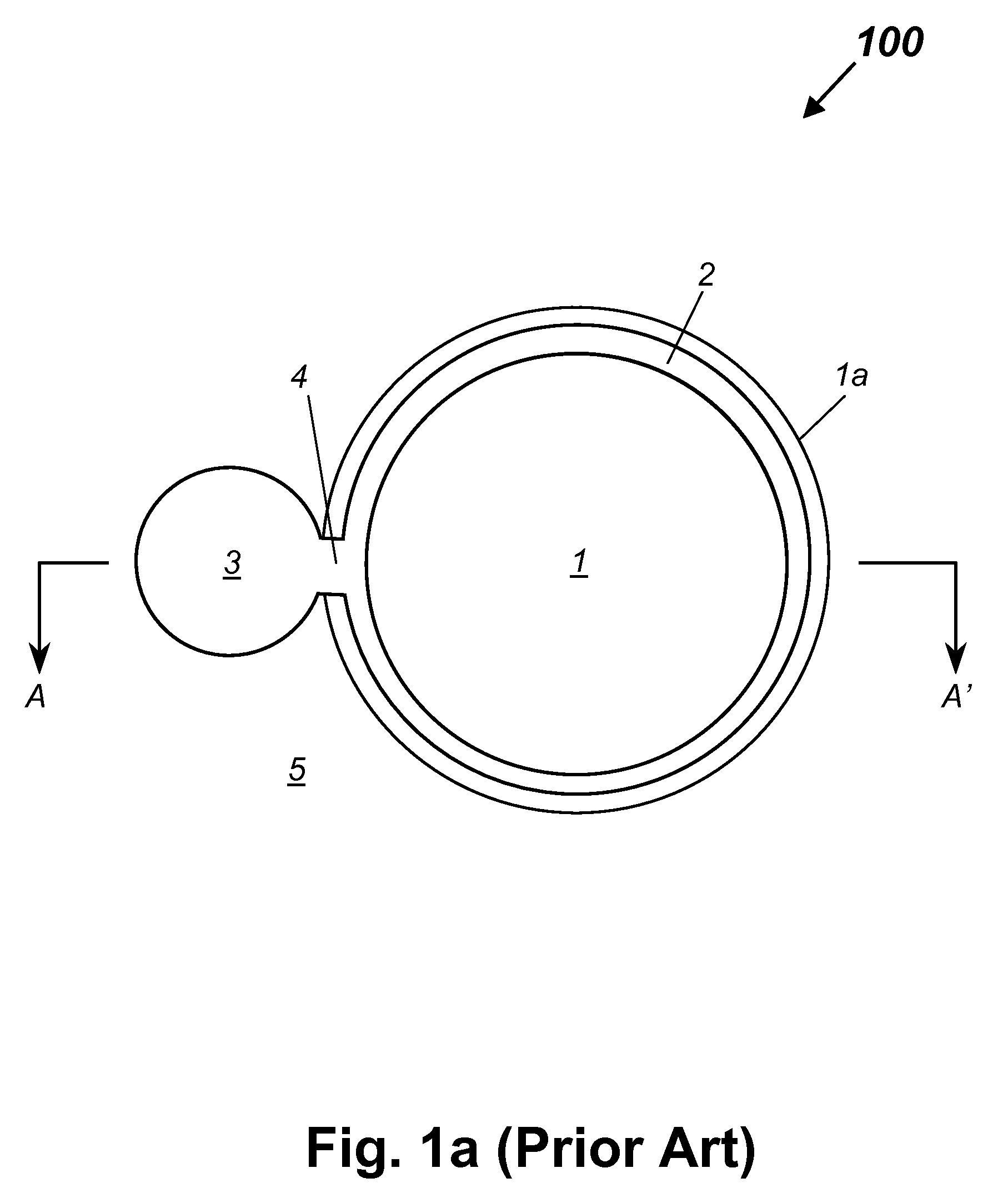
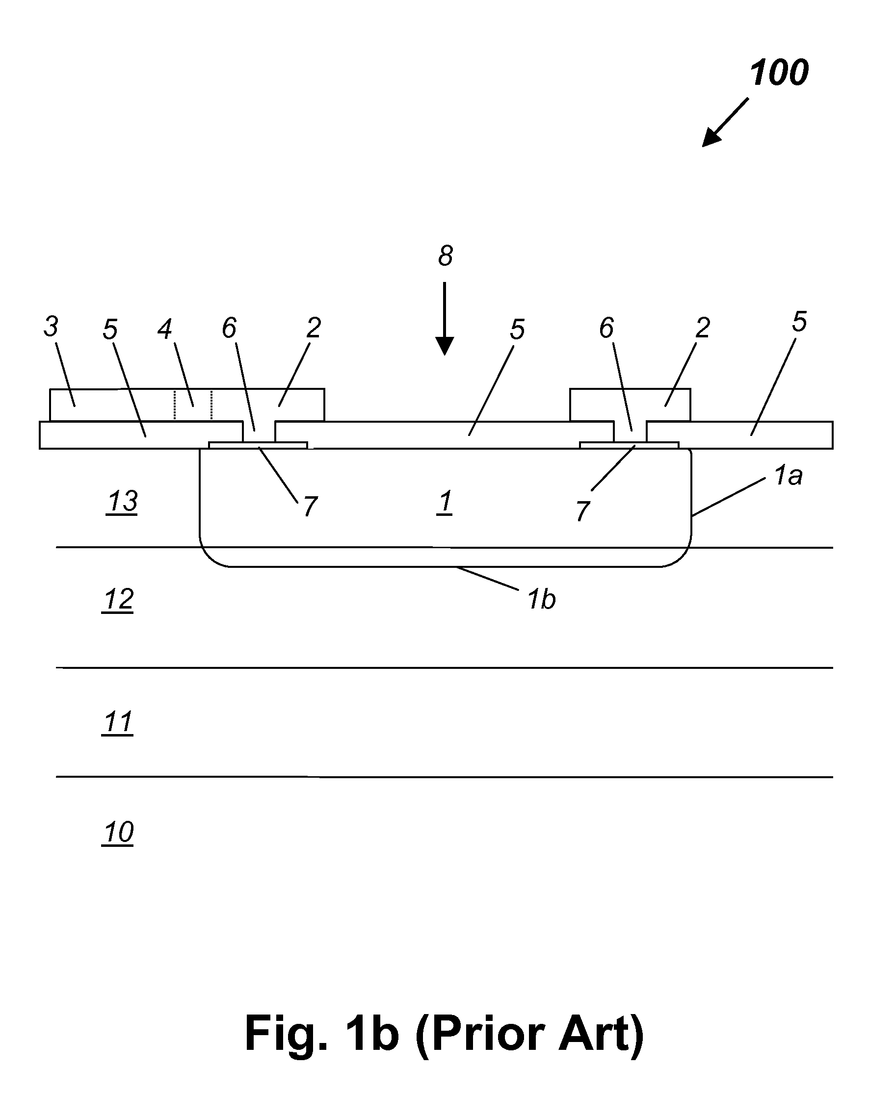
[0036]a p-i-n photodiode 200 is shown as a cross-section in FIG. 3a.

[0037]The p-i-n photodiode 200 a substrate 10 supports an n-type layer structure comprising a n-doped buffer layer 11 0.3-1.0 μm thick, an unintentionally doped absorption layer 12 0.8-4 μm thick, and a n-doped or unintentionally doped window layer 13. The window layer 13 may comprise a lowly doped p-type semiconductor layer with a p-doping level less than 1×1017 cm−3. Alternatively, it may comprise a compensated layer with high resistance, such as a grown-in n-type layer with a doping level in the range 1×10¹⁷ to 5×1017 cm−3. As the doping of this n-type layer is just slightly lower than the p-doping produced through a p-region diffusion process, it becomes a compensated layer after the p-region diffusion.

[0038]A p-n junction 1b is formed in the absorption layer 12 by a localized p-type dopant diffusion process to form the p-region 1 with periphery 1a. Typically zinc (Zn) is used as the p-type dopant for diffusion...

second embodiment

[0050]In a second embodiment, the photodiode 300 in FIG. 3b has the contact ring 2 directly contacting the InP window layer 13 within the p-region 1. For this purpose a gold-zinc (AuZn) layer 16 is substituted for the contact layer 7 of the previous embodiment. While the AuZn layer 16 forms an inferior ohmic contact to the InP window layer 13, it will be sufficiently good for high speed operation of the photodiode.

third embodiment

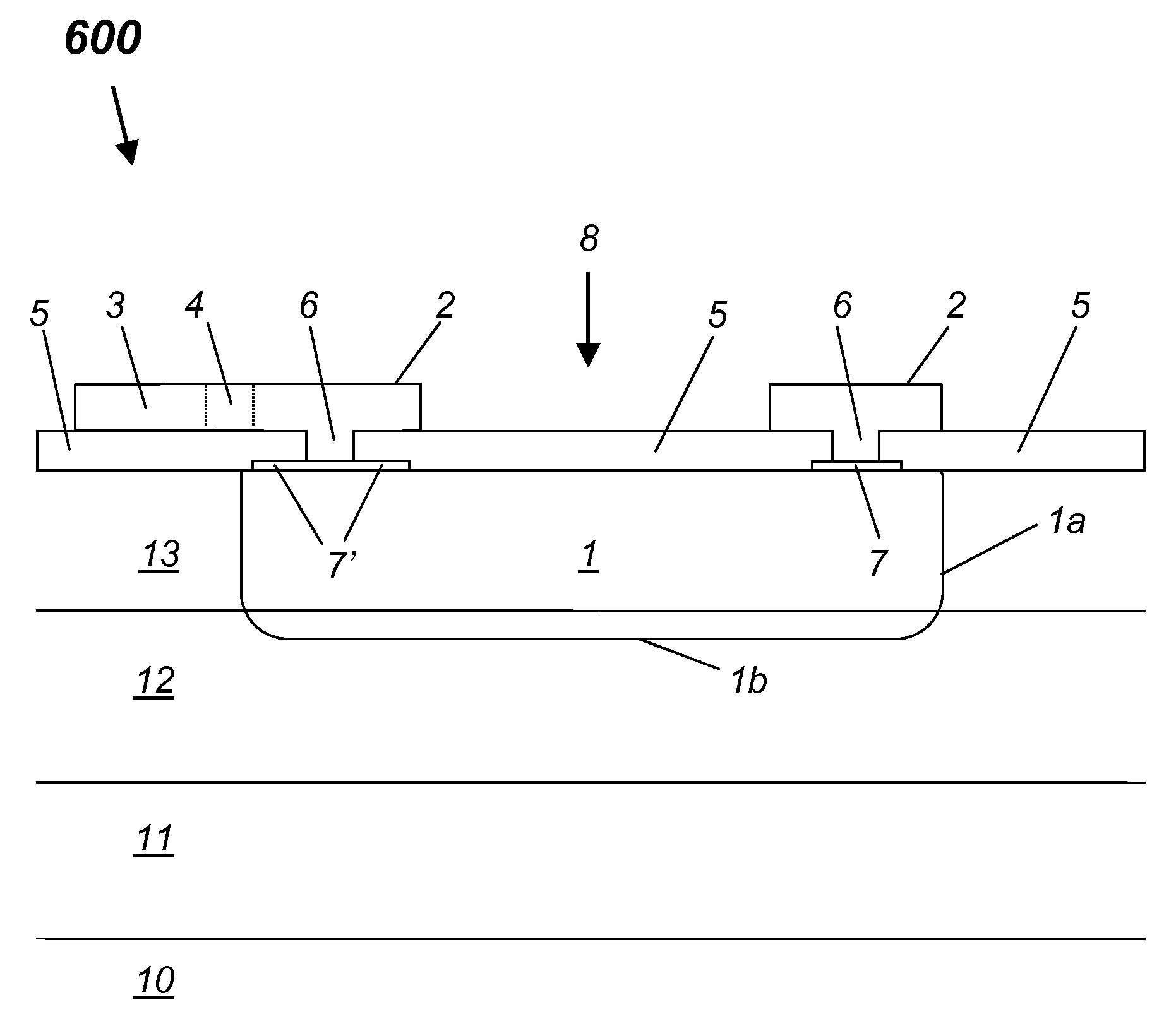
[0051]In a third embodiment, the photodiode 400 in FIG. 4 the window layer 13 of the previous embodiments is subdivided into a lower window layer 13, a current spreading layer 14 and an upper window layer 15. The lower and upper window layers 13 and 15 are either undoped or slightly n-doped to a level of 1×10¹⁶ to 5×1016 cm−3 to reduce a dark current of the photodiode 400.

[0052]In order to promote a lateral spreading of electrical current flowing from the contact ring 2 toward the buffer layer 11, the current spreading layer 14 is doped higher than the lower and upper window layers 13 and 15. For the current spreading layer 14, the doping level should be in the range of 1×10¹⁷ to 5×1017 cm−3, while the thickness should be about 0.2 to 0.5 micron.

[0053]To form the p-n junction 1b in the absorption layer 12, the localized p-type dopant diffusion (using, for instance, Zn) extends through the upper window layer 15, the current spreading layer 14 and the lower window layer 13. Within the...


PUM


Abstract

A photodetector with an improved electrostatic discharge damage threshold is disclosed, suitable for applications in telecommunication systems operating at elevated data rates. The photodetector may be a PIN or an APD fabricated in the InP compound semiconductor system. The increased ESD damage threshold is achieved by reducing the ESD induced current density in the photodetector by a suitable widening of the contact at a critical location, increasing the series resistance and promoting lateral current spreading by means of a current spreading layer.

Description

TECHNICAL FIELD[0001]The present invention relates to photodetectors, and more particularly, to their protection against electrostatic discharge.BACKGROUND OF THE INVENTION[0002]Photodiodes or photodetectors including PINs and avalanche photodiodes (APDs) are widely used in fiberoptic and optical applications to convert received light into an electrical current signal. The photodiodes require a fast response time to be able to operate in high speed data transmission systems.[0003]Photodiodes with a fast response time as used in such high speed signal transmission are especially vulnerable to damage from electrostatic discharge (ESD). The susceptibility of an electronic component to ESD is measured in terms of an ESD threshold. The higher the threshold, the more robust the component is against damage.[0004]Typically the bandwidth of a photodiode is limited by the product of its capacitance and series resistance, known as its RC constant. In most photodiodes the capacitance of the p-n...

Claims


Application Information

Patent Timeline
Patent Type & Authority Applications(United States)
IPC IPC(8): H01L31/105H01L31/0216
CPCH01L31/022416H01L31/105Y02E10/544H01L31/1844H01L31/107Y02E10/548
Inventor PAN, ZHONGVENABLES, DAVID
Owner LUMENTUM OPERATIONS LLC
Why Eureka
Try Eureka