Packaging substrate structure having semiconductor chip embedded therein and fabricating method thereof

a technology of semiconductor chips and packaging substrates, applied in the manufacture of printed circuits, basic electric elements, printed circuit stress/warp reduction, etc., can solve the problems of reduced transmitting efficiency, reduced and increased manufacturing costs, so as to reduce stress on the surface of semiconductor chips , the reliability of whole package structure can be increased, the effect of low yield of packaging substrates

Inactive Publication Date: 2009-04-02
PHOENIX PRECISION TECH CORP
View PDF8 Cites 37 Cited by
  • Summary
  • Abstract
  • Description
  • Claims
  • Application Information

AI Technical Summary

Benefits of technology

[0014]Namely, according to the packaging substrate structure having an semiconductor chip embedded therein and the method for manufacturing the same of the present invention, the number of layers of the built-up structure disposed in the upper position of the semiconductor chip of the packaging substrate structure is less than that of the conventional packaging substrate structure. As a result, the stress imposed on the surface of the semiconductor chip can be reduced and the reliability of the whole package structure can be increased. Besides, the problem of the low yield of the packaging substrate due to the increasing number of layers, that further causes scrapping of the good chips embedded in the substrate, can be avoided. Also, the transmiting efficiency is enhanced because of the shortening of the transmiting path, and noise interference is diminished so as to enhance electrical quality.

Problems solved by technology

The more the layers of the built-up structure, the larger the stress imposed on the chip, thereby the reliability of the whole package structure is weakened.
Besides, if the yield of the packaging substrate decreases caused by the increasing number of layers, more good chips embedded in the substrate will be compromised, which means a higher manufacturing cost will be incurred.
Also, the transmiting efficiency is reduced because of the long transmiting path owing to the numerous built-up substrates disposed on the chip, and noise interference is increased leading to a drop in the electrical quality.

Method used


Image

  • Packaging substrate structure having semiconductor chip embedded therein and fabricating method thereof
  • Packaging substrate structure having semiconductor chip embedded therein and fabricating method thereof
  • Packaging substrate structure having semiconductor chip embedded therein and fabricating method thereof

Examples


example 1

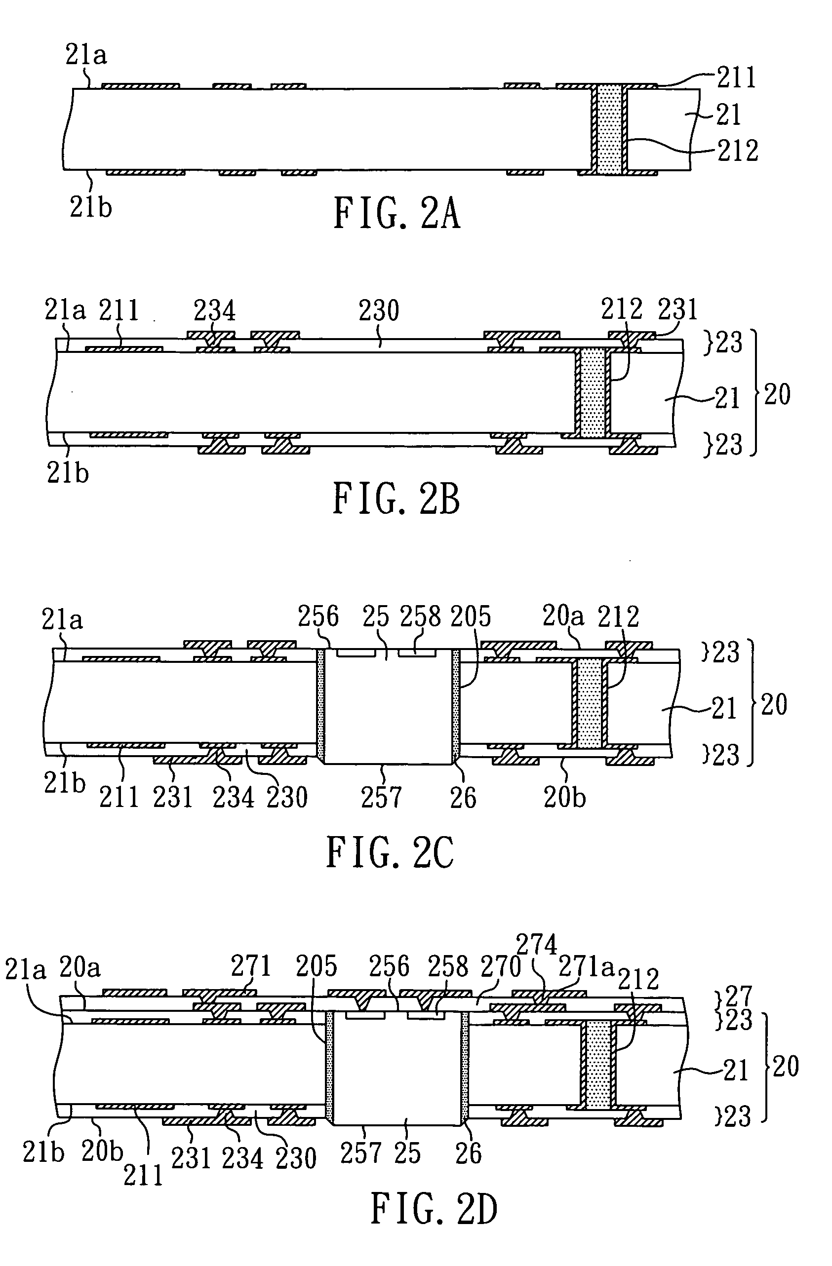
[0020]With reference to FIGS. 2A to 2E′, there is shown a flow chart for manufacturing a packaging substrate structure having an semiconductor chip embedded therein in the present example.

[0021]As shown in FIG. 2A, a core board 21 is provided first. This core board 21 has wiring layers 211 disposed on the surface of the core board 21 and a conductive through hole 212 extending through the core board 21. The two wiring layers 211 disposed respectively on the two surfaces 21a, 21b of the core board 21 are electrically connected to each other by the conductive through hole 212.

[0022]Then as shown in FIG. 2B, a first built-up structure 23 is formed on each surface of the core board 21 together with the wiring layer 211. The first built-up structure 23 has at least one first dielectric layer 230, at least one first wiring layer 231 disposed on the first dielectric layer 230, and a plurality of first conductive vias 234 electrically connecting to the first wiring layer 231.

[0023]The metho...

example 2

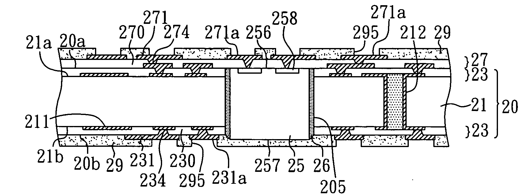
[0030]In reference with FIGS. 3A to 3E′, the flow chart for manufacturing a packaging substrate structure having an semiconductor chip embedded therein in the present example is shown. The method of the present example is the same as that of Example 1, except that, after the formation of the first built-up structure 23 and embedding of the semiconductor chip 25, a second built-up structure 27 is additionally formed on the inactive surface 257 of the semiconductor chip 25 as well as the surface 20b of the substrate body 20, as represented in FIG. 3D. Further, a conductive through hole 232 is formed through the substrate body 20 except the conductive through hole 212. With reference to FIG. 3E and 3E′, a solder mask 29 is formed covering one surface 20a (having no second built-up structure 27 thereon) of the substrate body 20 and covering the active surface 256 of the semiconductor chip 25, in which a plurality of openings 295 are formed in the solder mask 29 to expose the electrode p...

example 3

[0031]In reference with FIGS. 4A to 4E′, the flow chart for manufacturing a packaging substrate structure having an semiconductor chip embedded therein in the present example is shown. The difference between the present example and the previous two examples is that the second built-up structure 27 is formed on each of the opposite surfaces 20a and 20b of the substrate body 20 as shown in FIG. 4D. The process steps of providing the packaging substrate structure of the present example are reference to those of Example 1, which are not further discussed here.

[0032]As mentioned above, according to the packaging substrate structure having an semiconductor chip embedded therein and the method for manufacturing the same of the present invention, the number of layers of the built-up structure disposed in the upper position of the semiconductor chip of the packaging substrate structure is fewer than those of the conventional packaging substrate structure. As a result, the stress imposed on t...


PUM


Abstract

The present invention relates to a packaging substrate structure having an semiconductor chip embedded therein and a method for manufacturing the same. The structure comprises: a substrate body having a through cavity, wherein the substrate body is a multilayer board which comprises a core board and a first built-up structure disposed on each of the opposite surfaces of the core board; an semiconductor chip disposed and fixed in the cavity, wherein the active surface of the semiconductor chip has a plurality of electrode pads thereon; and a second built-up structure disposed on at least one surface of the substrate body as well as the surface of the semiconductor chip, wherein the second built-up structure has a plurality of conductive vias conducting to the first built-up structure. The present invention can reduce the stress imposed on the surface of the semiconductor chip and increase the reliability of the whole package structure.

Description

BACKGROUND OF THE INVENTION[0001]1. Field of the Invention[0002]The present invention relates to a packaging substrate structure having an semiconductor chip embedded therein and a method for manufacturing the same and, particularly relates to a packaging substrate structure with an semiconductor chip embedded therein having improved yield and a method for manufacturing the same.[0003]2. Description of Related Art[0004]Customer demands of the electronics industry continue to evolve rapidly and the main trends are high integration and miniaturization. In order to satisfy those requirements, especially in the packaging of semiconductor devices, development of circuit boards with the maximum of active and passive components and conductive wires has progressed from single to multiple layer types. This means that a greater circuit layout area is available due to interlayer connection technology. Accordingly, more circuits and electronic components per unit volume of the packaging substra...

Claims


Application Information

Patent Timeline
Patent Type & Authority Applications(United States)
IPC IPC(8): H01L23/485H01L21/58
CPCH01L23/49827H01L23/5389H01L24/24H01L24/82H01L2224/24227H01L2924/01082H01L2924/01033H05K1/0271H05K1/185H05K3/4602H05K2203/1469H05K2203/1476H01L2924/18162
Inventor HSU, SHIH-PINGCHEN, SHANG-WEI
Owner PHOENIX PRECISION TECH CORP
Why Eureka
Try Eureka