LED device having improved light output

a technology of led devices and light output, which is applied in the manufacture of electrode systems, electric discharge tubes/lamps, and discharge tubes luminescnet screens, etc., can solve the problems of reducing device efficiency, difficult to scale to large substrates, and patterned organic material deposition technology, so as to increase the light output and manufacturability of led devices, and reduce any angular color change

Active Publication Date: 2009-04-02
GLOBAL OLED TECH
View PDF14 Cites 65 Cited by
  • Summary
  • Abstract
  • Description
  • Claims
  • Application Information

AI Technical Summary

Benefits of technology

[0013]The present invention has the advantage that it increases the light output and manufacturability of an LED device, and reduces any angular color change.

Problems solved by technology

Because LED devices employ high-optical-index emissive materials, a large fraction (e.g. greater than 50%) of the emitted light is trapped in the device due to total internal reflection and thus reduces the device efficiency.
While such designs are useful, they require a patterned organic material deposition technology (for example, vacuum deposition through metal shadow-masks) that is difficult to scale to large substrates.
Moreover, optical cavity devices typically suffer from an unacceptable angular color dependence.
However, while useful, such an approach does not improve the manufacturability of the device and provides inadequate ambient contrast ratio under some illumination conditions.
Moreover, the color filters absorb light emitted from the light-emitting layer, thereby reducing device efficiency.
Such designs, however, may have increased manufacturing costs, lower light output than desired, and reflectance larger than may be desired, as well as significant color change at different viewing angles, owing to the change in the effective optical path length for light traveling at angles to the normal.
Again such designs may have increased manufacturing costs due to patterned deposition processes.
Also, significant light may be absorbed by the color filters thereby reducing efficiency.
However, the use of color filters substantially reduces the efficiency of the device.
However, this disclosure does not address angular color issues or the large amount of trapped light.
However, this design employs a patterned semi-transparent electrode to form the white subpixel that can be difficult to manufacture in a top-emitting format.
Moreover, angular color change is not addressed in the patent.

Method used


Image

  • LED device having improved light output
  • LED device having improved light output
  • LED device having improved light output

Examples


Embodiment Construction

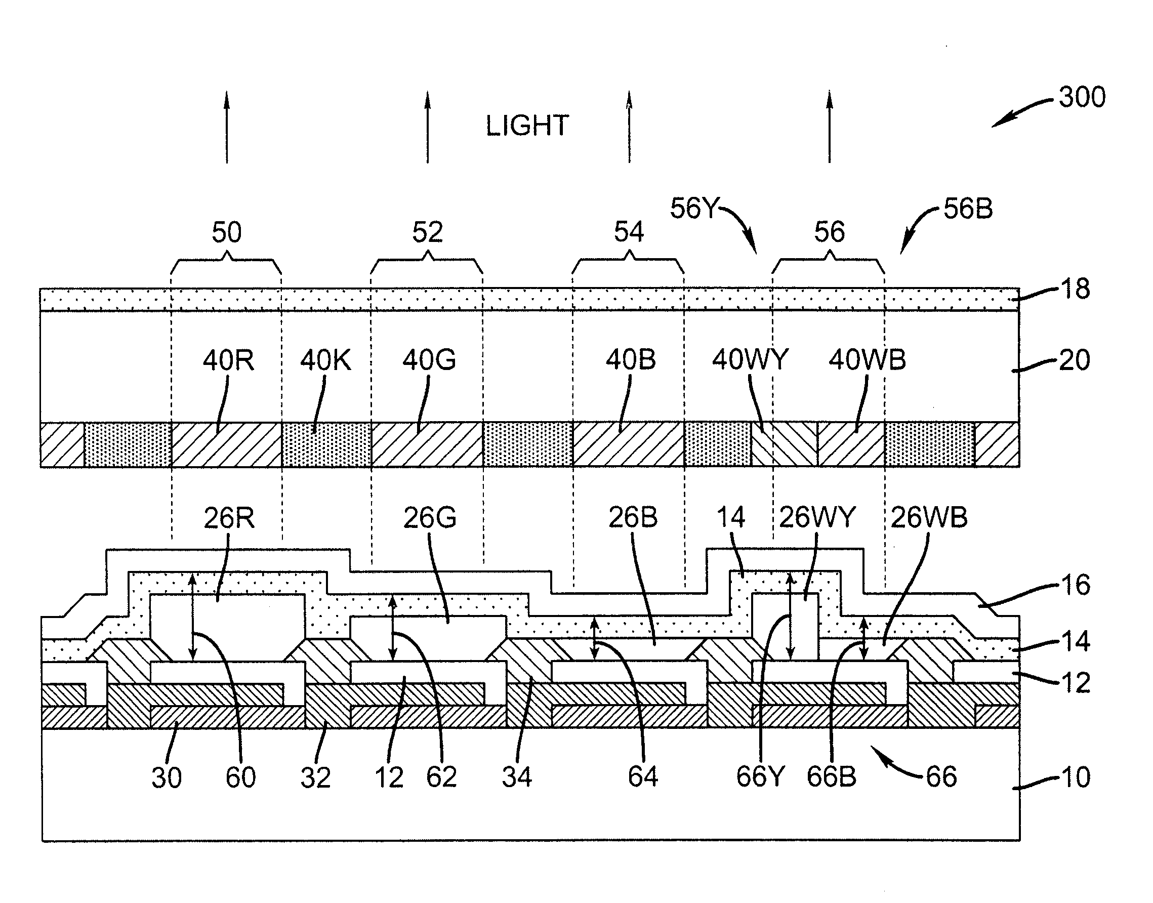
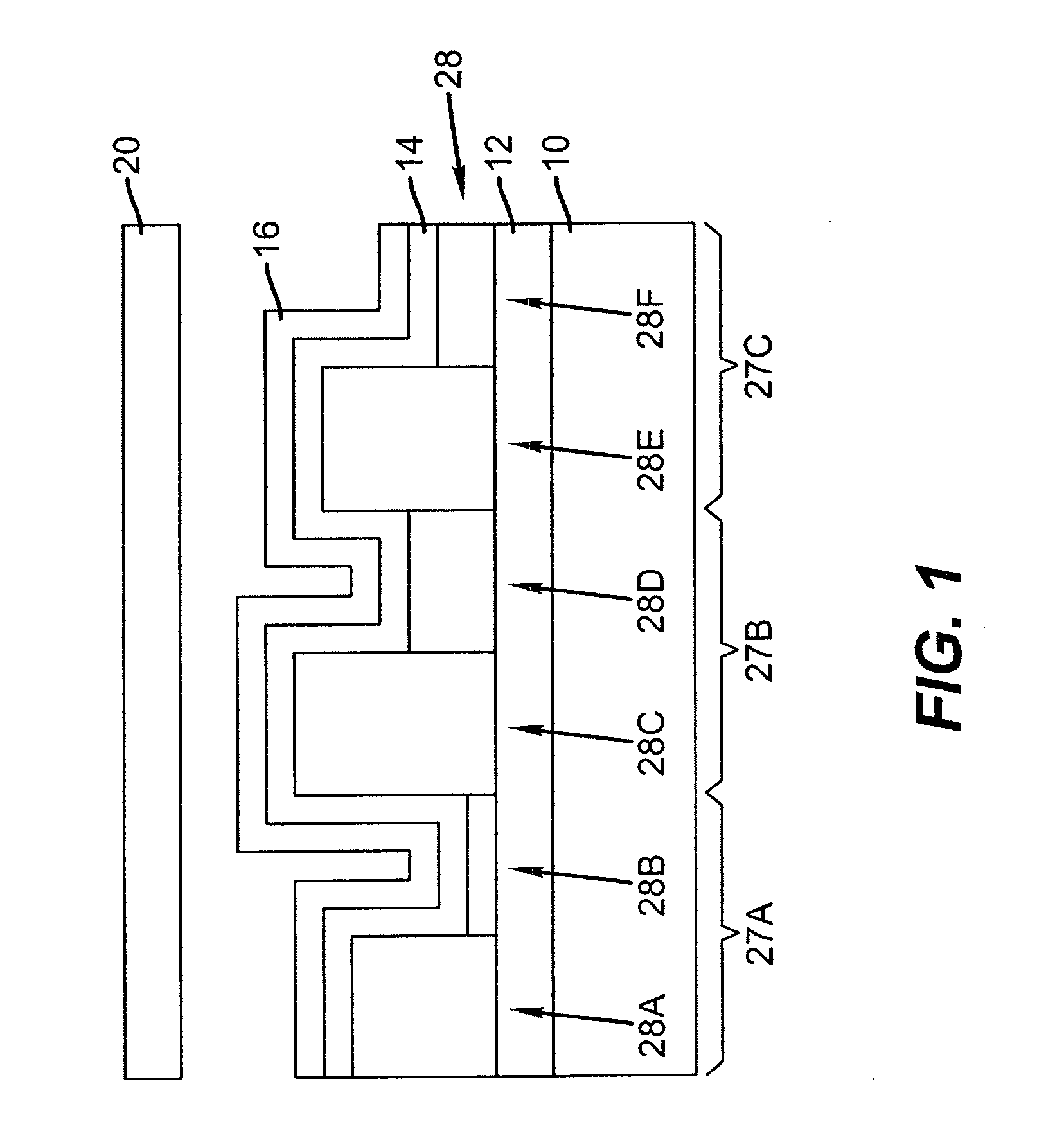
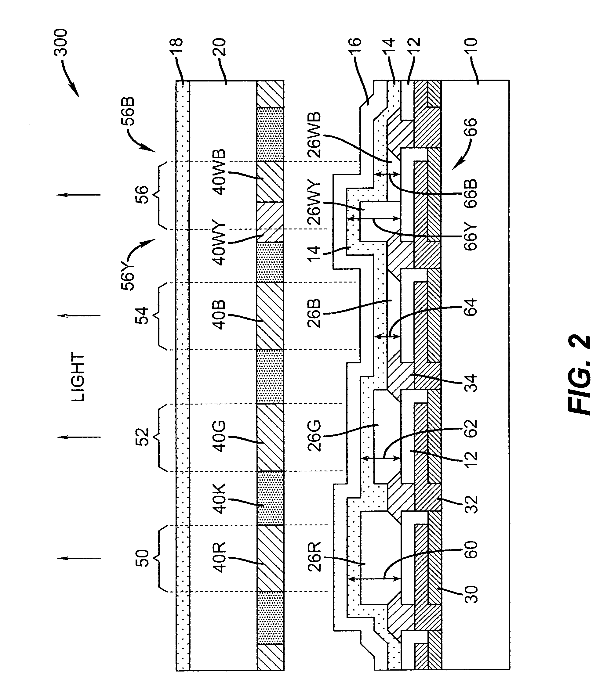
[0028]Referring to FIG. 1, a thin-film, white-light-emitting diode device according to the present invention, comprises a reflective, conductive thin-film structure 12 and a semi-transparent, conductive thin-film structure 16. One or more thin-film layers 14 are formed between the reflective and semi-transparent conductive thin-film structures thereby forming two or more commonly-controlled microcavity structures 28. The thin-film layers 14 emit white light in response to current provided by the conductive thin-film structures 12, 16. Each of the two or more microcavity structures 28 emits light having a smaller spectral range than the spectral range of the white-light-emitting thin-film layer(s) 14. The combination of light emitted by the microcavity structures 28 is white. The color change of the combined light emitted by the microcavity structures 28 over a range of angles is less than the color change of the light emitted by at least one of the microcavity structures 28 over the...


PUM


Abstract

A thin-film, white-light-emitting diode device includes a reflective, conductive thin-film structure and a semi-transparent, conductive thin-film structure. One or more thin-film layers are formed between the reflective and semi-transparent conductive thin-film structures to form two or more commonly-controlled microcavity structures. The thin-film layers emit white light in response to current provided by the conductive thin-film structure. Each of the two or more commonly-controlled microcavity structures has a different resonant frequency within one or more optical cavities and emits light with a smaller spectral range than the spectral range of the white-light-emitting thin-film layer(s). A combination of light emitted from the two or more commonly-controlled microcavity structures is white.

Description

FIELD OF THE INVENTION[0001]The present invention relates to light-emitting diode (LED) devices, and more particularly, to LED device structures for improving light output, manufacturability, and angular performance.BACKGROUND OF THE INVENTION[0002]Emissive flat-panel display devices are widely used in conjunction with computing devices and in particular with portable devices. These displays are often used in public areas with significant ambient illumination and are viewed from a wide variety of angles. Such devices are also under development as area illumination devices or lamps.[0003]Light emitting diodes (LED) incorporating thin films of light-emitting materials have many advantages in a flat-panel display device and are useful in optical systems. Such films can comprise either or both organic and inorganic materials. U.S. Pat. No. 6,384,529 issued May 7, 2002 to Tang et al. shows an OLED color display that includes an array of OLED light emitting elements (pixels). Light is emi...

Claims


Application Information

Patent Timeline
Patent Type & Authority Applications(United States)
IPC IPC(8): H01J1/62H01J9/02
CPCH01L27/3211H01L27/3213H01L2251/5361H01L51/5265H01L51/5036H10K59/351H10K50/125H10K50/852H10K59/35
Inventor COK, RONALD S.MILLER, MICHAEL E.
Owner GLOBAL OLED TECH
Why Eureka
Try Eureka