Void-free copper filling of recessed features for semiconductor devices

a technology of semiconductor devices and recessed features, applied in semiconductor/solid-state device manufacturing, basic electric elements, electric devices, etc., can solve the problems of voids in bulk metal filling of recessed features, recessed features are becoming so small, and open and extruded metal lines

Active Publication Date: 2009-04-02
TOKYO ELECTRON LTD
View PDF58 Cites 40 Cited by
  • Summary
  • Abstract
  • Description
  • Claims
  • Application Information

AI Technical Summary

Benefits of technology

[0009]According to one embodiment of the invention, the method includes providing a patterned substrate containing a recessed feature, depositing a barrier film on the substrate, including in the recessed feature, depositing a Ru metal film on the barrier film, depositing a discontinuous Cu seed layer on the Ru metal film, the discontinuous Cu seed layer partially covering the Ru metal film in the recessed feature. The method further includes exposing the substrate to an oxidation source gas that oxidizes the Cu seed layer and a portion of the Ru metal film not covered by the Cu seed layer, heat-treating the oxidized Cu seed layer and the oxidized portion of the Ru metal film under high vacuum conditions or in the presence of an inert gas but not H2 gas to activate the oxidized portion of the Ru metal film for Cu plating, and filling the recessed feature with bulk Cu metal.

Problems solved by technology

For example, the recessed features are becoming so small that voids in bulk metal filling of the recessed features are unacceptable.
As the width of metal lines are scaled down to smaller submicron and even nanometer dimensions, electromigration failure, which may lead to open and extruded metal lines, is now a well-recognized problem.
Moreover, as dimensions of metal lines further decrease, metal line resistivity increases substantially, and this increase in line resistivity may adversely affect circuit performance.
However, Cu metal cannot be put in direct contact with dielectric materials since Cu metal has poor adhesion to the dielectric materials and Cu is known to easily diffuse into common integrated circuit materials such as silicon and dielectric materials where Cu is a mid-bandgap impurity.
Furthermore, oxygen can diffuse from an oxygen-containing dielectric material into Cu, thereby decreasing the electrical conductivity of the Cu metal.
However, Ta is normally deposited by sputtering or plasma processing methods which are unable to provide conformal coverage over high aspect ratio recessed features.
However, Cu metallization structures containing Ru metal films have generally showed higher Cu resistivity than those containing the traditional TaN / Ta bilayers and oxidation of the Ru metal films during processing can result in voids and incomplete bulk Cu metal fill in the recessed features, thereby increasing the electrical resistance and adversely affecting the reliability of the semiconductor device.

Method used


Image

  • Void-free copper filling of recessed features for semiconductor devices
  • Void-free copper filling of recessed features for semiconductor devices
  • Void-free copper filling of recessed features for semiconductor devices

Examples


Embodiment Construction

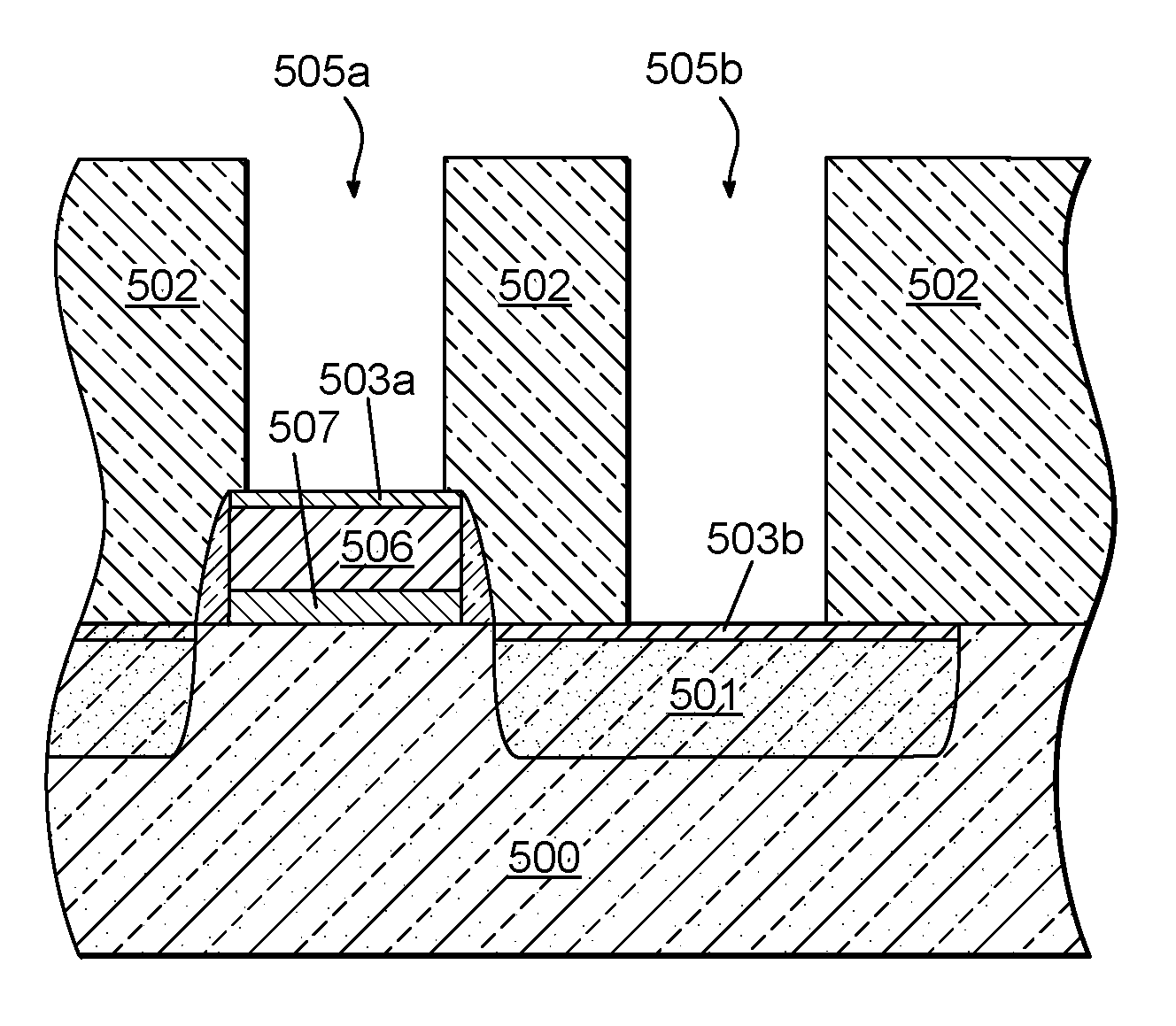
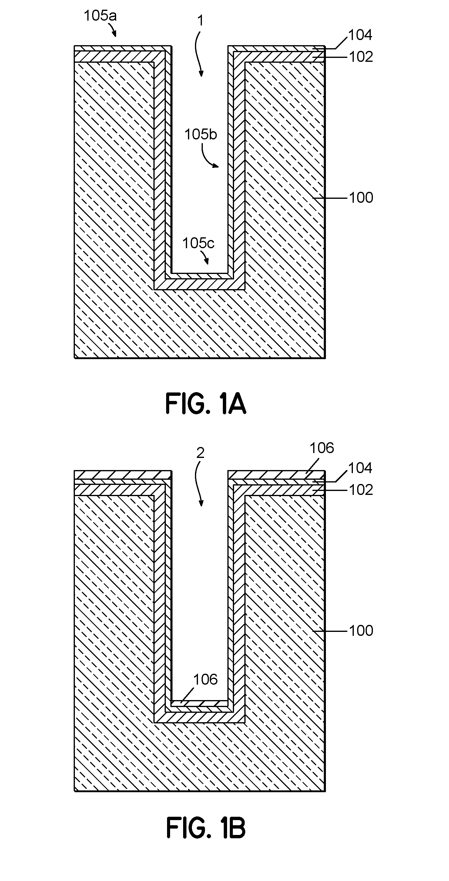
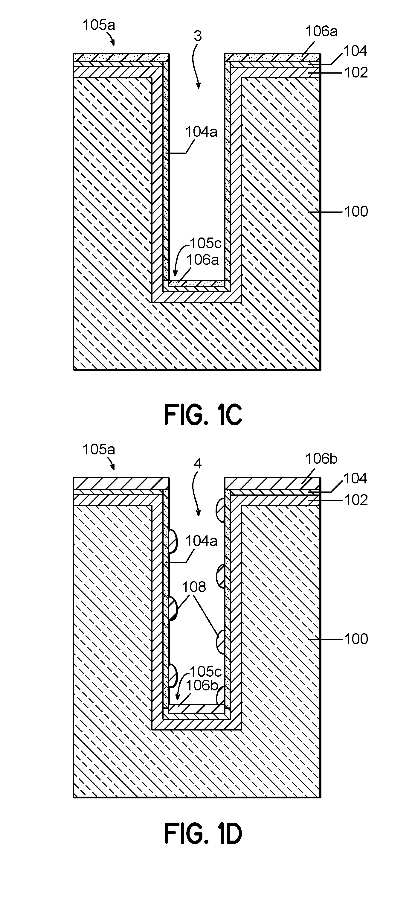
[0018]Method for void-free Cu filling of recessed features in semiconductor devices is disclosed in several embodiments. The current inventors have studied different process variations and heat-treating processes that affect Cu voiding in recessed features containing a barrier film, a conformal Ru metal film on the barrier film, and bulk Cu metal filling the recessed feature. Cu voiding is a problem that is encountered due to oxidation of the Ru metal film during air exposure of about 2 hours or more prior to bulk Cu metal filling using a Cu plating process. Such air exposure is common in device manufacturing environments. Embodiments of the invention enable device manufacturers to integrate Ru metal films with void-free Cu filling of the recessed features. The Ru metal films can be deposited with excellent conformality and can provide greatly improved bulk Cu metal filling of high-aspect ratio recessed features.

[0019]One skilled in the relevant art will recognize that the various e...


PUM

PropertyMeasurementUnit
temperatureaaaaaaaaaa
widthaaaaaaaaaa

Abstract

A method is provided for void-free copper (Cu) filling of recessed features in a semiconductor device. The method includes providing a patterned substrate containing a recessed feature, depositing a barrier film on the patterned substrate, including in the recessed feature, depositing a Ru metal film on the barrier film, and depositing a discontinuous Cu seed layer on the Ru metal film, where the Cu seed layer partially covers the Ru metal film in the recessed feature. The method further includes exposing the substrate to an oxidation source gas that oxidizes the Cu seed layer and the portion of the Ru metal film not covered by the Cu seed layer, heat-treating the oxidized Cu seed layer and the oxidized Ru metal film under high vacuum conditions or in the presence of an inert gas to activate the oxidized Ru metal film for Cu plating, and filling the recessed feature with bulk Cu metal. The exposure to the oxidation source gas can be an air exposure commonly encountered in semiconductor device manufacturing prior to Cu plating.

Description

CROSS REFERENCE TO RELATED APPLICATIONS[0001]The present invention is related to U.S. patent application Ser. No. 10 / 693,298, filed Mar. 29, 2007 and entitled METHOD OF FORMING LOW-RESISTIVITY COPPER FILM STRUCTURES, the entire content of which is incorporated herein by reference in its entirety.FIELD OF THE INVENTION[0002]The invention relates to semiconductor devices, and more particularly to processing methods for void-free copper (Cu) filling of recessed features containing a ruthenium (Ru) film.BACKGROUND OF THE INVENTION[0003]An integrated circuit contains various semiconductor devices and a plurality of conducting metal paths that provide electrical power to the semiconductor devices and allow these semiconductor devices to share and exchange information. Within an integrated circuit, metal layers are stacked on top of one another using intermetal or interlayer dielectric layers that insulate the metal layers from each other. Normally, each metal layer must form an electrical...

Claims


Application Information

Patent Timeline
Patent Type & Authority Applications(United States)
IPC IPC(8): H01L21/4763
CPCH01L21/28518H01L21/2855H01L21/28556H01L21/76843H01L21/76844H01L21/76883H01L21/76864H01L21/76868H01L21/76873H01L21/76874H01L21/76862
Inventor SUZUKI, KENJIISHIZAKA, TADAHIROJOMEN, MIHORULLAN, JONATHAN
Owner TOKYO ELECTRON LTD
Why Eureka
Try Eureka