Stacked semiconductor device and fabricating method thereof

a technology of semiconductor devices and stacked semiconductors, applied in the direction of solid-state devices, printed circuit components, basic electric elements, etc., can solve the problems of unfavorable great height of conventional stacked semiconductor devices and the fabrication process, and achieve the reduction of package height and package miniaturization, simplifying the fabrication process, and reducing costs

Active Publication Date: 2009-04-09
UNIMICRON TECH CORP
View PDF6 Cites 41 Cited by
  • Summary
  • Abstract
  • Description
  • Claims
  • Application Information

AI Technical Summary

Benefits of technology

[0021]The present invention provides a stacked semiconductor device and a method for fabricating the same. The method comprises the steps of: sandwiching at least two semiconductor chips in between a first flexible layer and a second flexible layer combined together to serve as a flexible substrate body with the semiconductor chips embedded therein, wherein a first circuit layer is formed on the second flexible layer and electrically connected to the semiconductor chips; bending th

Problems solved by technology

Accordingly, an issue that calls for immediate solution involves solving the drawbacks of the prior art, namely un

Method used


Image

  • Stacked semiconductor device and fabricating method thereof
  • Stacked semiconductor device and fabricating method thereof
  • Stacked semiconductor device and fabricating method thereof

Examples


first embodiment

[0028]FIGS. 2A through 2K are cross-sectional views of a stacked semiconductor device and a method for fabricating the same according to the present invention.

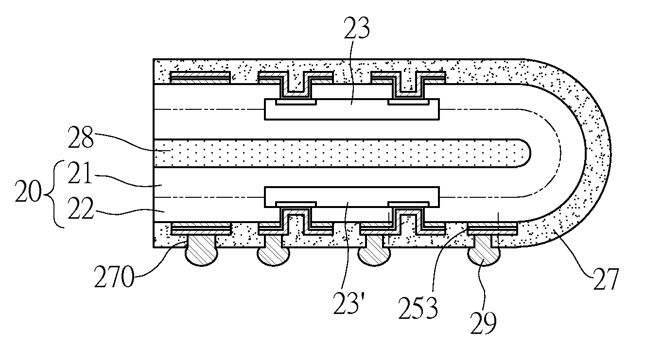
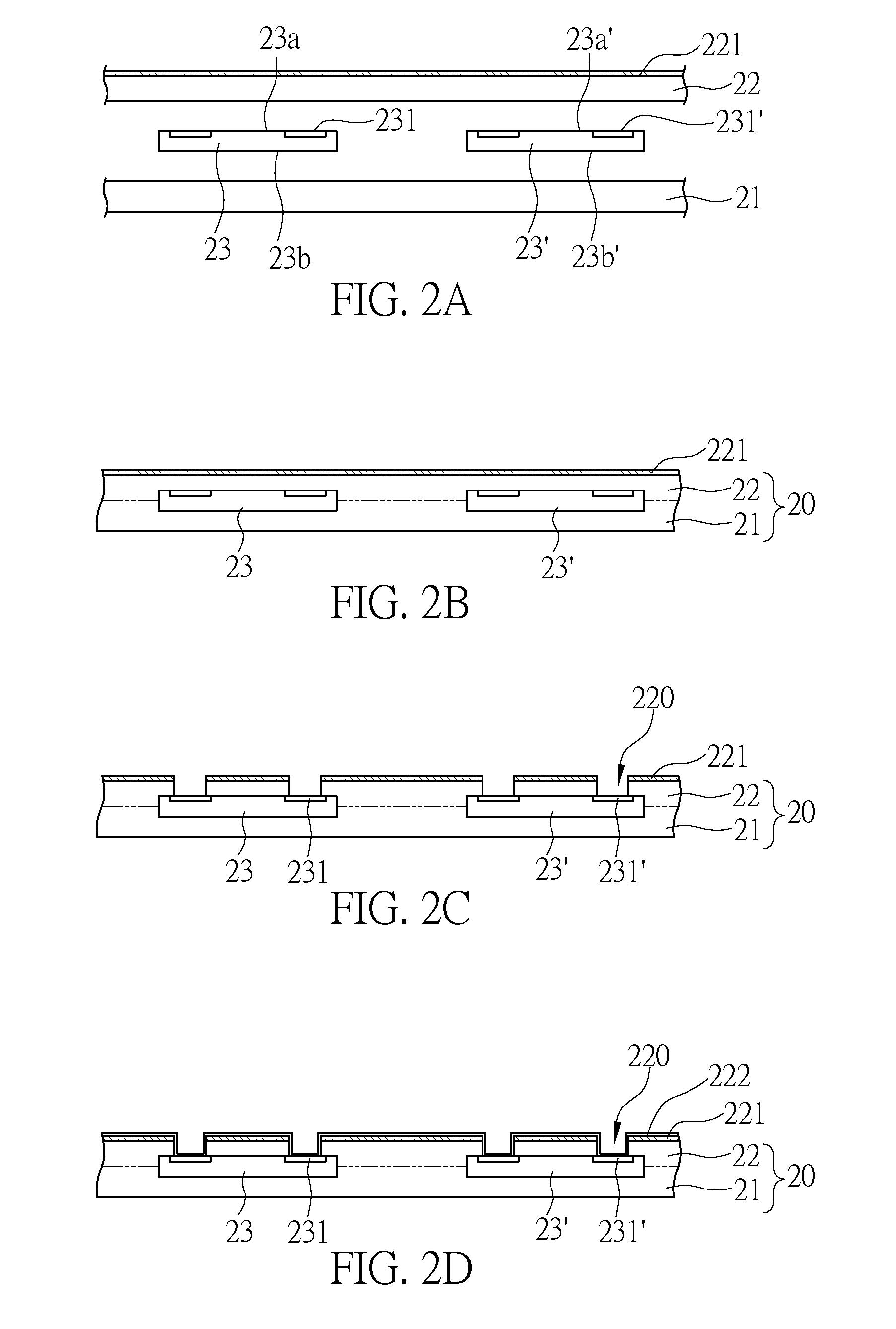
[0029]Referring to FIG. 2A, a first flexible layer 21 and a second flexible layer 22 and at least two semiconductor chips 23, 23′ are provided. A metal layer 221 is formed on the second flexible layer 22. Each of the semiconductor chips 23, 23′ has an active surface 23a, 23a′ with a plurality of electrode pads 231, 231′ thereon and an opposing inactive surface 23b, 23b′.

[0030]Referring to FIG. 2B, the semiconductor chips 23, 23′ are each sandwiched in between the first and second flexible layers 21, 22, then the first and second flexible layers 21, 22 are combined together to serve as a flexible substrate body 20 with the semiconductor chips 23, 23′ embedded therein.

[0031]Referring to FIG. 2C, a plurality of vias 220 are formed in the second flexible layer 22 and the metal layer 221 thereon so as to expose a portion of the el...

second embodiment

[0046]FIGS. 3A through 3C are cross-sectional views of a second embodiment of a stacked semiconductor device and a method for fabricating the same according to the present invention. Unlike the first embodiment, the second embodiment teaches forming the first circuit layer by electroplating.

[0047]Referring to FIG. 3A, like what is shown in FIG. 2D, the plurality of vias 220 are formed in the second flexible layer 22 and the metal layer 221 thereon so as to expose portions of the electrode pads 231, 231′ on the semiconductor chips 23, 23′ sandwiched in between the first and second flexible layers 21, 22. The conductive layer 222 is formed on the metal layer 221, surfaces of the vias 220, and a portion of the electrode pads 231, 231′. The resist layer 24 is formed on the conductive layer 222. A plurality of open areas 240 are formed in the resist layer 24 so as to expose parts of the conductive layer 222.

[0048]Referring to FIG. 3B, the electroplated metal layer 223 is formed on the co...


PUM


Abstract

Provided is a stacked semiconductor device including a first flexible layer and a second flexible layer combined together, serving as a flexible substrate body being bent somewhere such that a surface of the first flexible layer itself is face-to-face clipped, two semiconductor chips each embedded in the flexible substrate body, and an adhesive layer sandwiched in a gap between the face-to-face surface of the first flexible layer. The active surface of each of the semiconductor chips has plurality of electrode pads thereon electrically connected to a first circuit layer on the second flexible layer. The semiconductor chips are stacked up and embedded in the flexible substrate body, thereby reducing package height to achieve miniaturization of electronic products. A method for fabricating the stacked semiconductor device is also provided.

Description

BACKGROUND OF THE INVENTION[0001]1. Field of the Invention[0002]The present invention relates to stacked semiconductor devices and methods for fabricating the same, and more particularly, to a stacked semiconductor device and a method for fabricating the same, wherein the method comprises bending and stacking up semiconductor chip-embedded flexible packaging substrates.[0003]2. Description of the Prior Art[0004]Owing to development of semiconductor packaging technology, semiconductor packages nowadays come in a variety of forms. Known methods for packaging semiconductor devices involve mounting an integrated circuit-laden semiconductor chip on a packaging substrate or a lead frame, electrically connecting the semiconductor chip to the packaging substrate or the lead frame, and encapsulating the packaging substrate with encapsulant. Known semiconductor packages are typically modularized using multi-chip module (MCM) in order to enhance electrical functions of a semiconductor chip, me...

Claims


Application Information

Patent Timeline
IPC IPC(8): H01L21/58H01L23/12
CPCH01L23/5387H01L2924/01033H01L24/19H01L25/0657H01L2224/04105H01L2224/20H01L2224/48091H01L2224/73265H01L2225/06517H01L2225/06524H01L2225/06572H01L2924/01078H01L2924/01082H01L2924/14H05K1/185H05K1/188H05K1/189H05K2201/055H05K2201/09509H05K2201/10674H01L23/5389H01L24/48H01L2924/00014H01L2224/451H01L24/45H01L2924/181H01L2224/12105H01L2924/00015H01L2224/05599H01L2924/00012
Inventor CHIA, KAN-JUNG
Owner UNIMICRON TECH CORP
Why Eureka
Try Eureka