Nonvolatile memories which combine a dielectric, charge-trapping layer with a floating gate

a charge-trapping layer and non-volatile memory technology, applied in the direction of semiconductor devices, electrical apparatus, transistors, etc., can solve the problem of memory becoming more difficult to fabricate, and achieve the effect of reducing the thickness of the floating gate and enhancing the charge storage capacity of the charge-trapping layer

Inactive Publication Date: 2009-04-16
PROMOS TECH PTE LTD
View PDF10 Cites 216 Cited by
  • Summary
  • Abstract
  • Description
  • Claims
  • Application Information

AI Technical Summary

Benefits of technology

[0005]In some embodiments of the present invention, the charge storage element includes both a charge trapping layer and a conductive layer (i.e. a floating gate). The floating gate serves

Problems solved by technology

This large thickness is an impediment to scaling the memory area because the thickness-to-width ratio of th

Method used


Image

  • Nonvolatile memories which combine a dielectric, charge-trapping layer with a floating gate
  • Nonvolatile memories which combine a dielectric, charge-trapping layer with a floating gate

Examples


Embodiment Construction

[0012]The embodiments described in this section illustrate but do not limit the invention. In particular, the invention is not limited to specific dimensions, materials, or modes of operation except as defined by the appended claims.

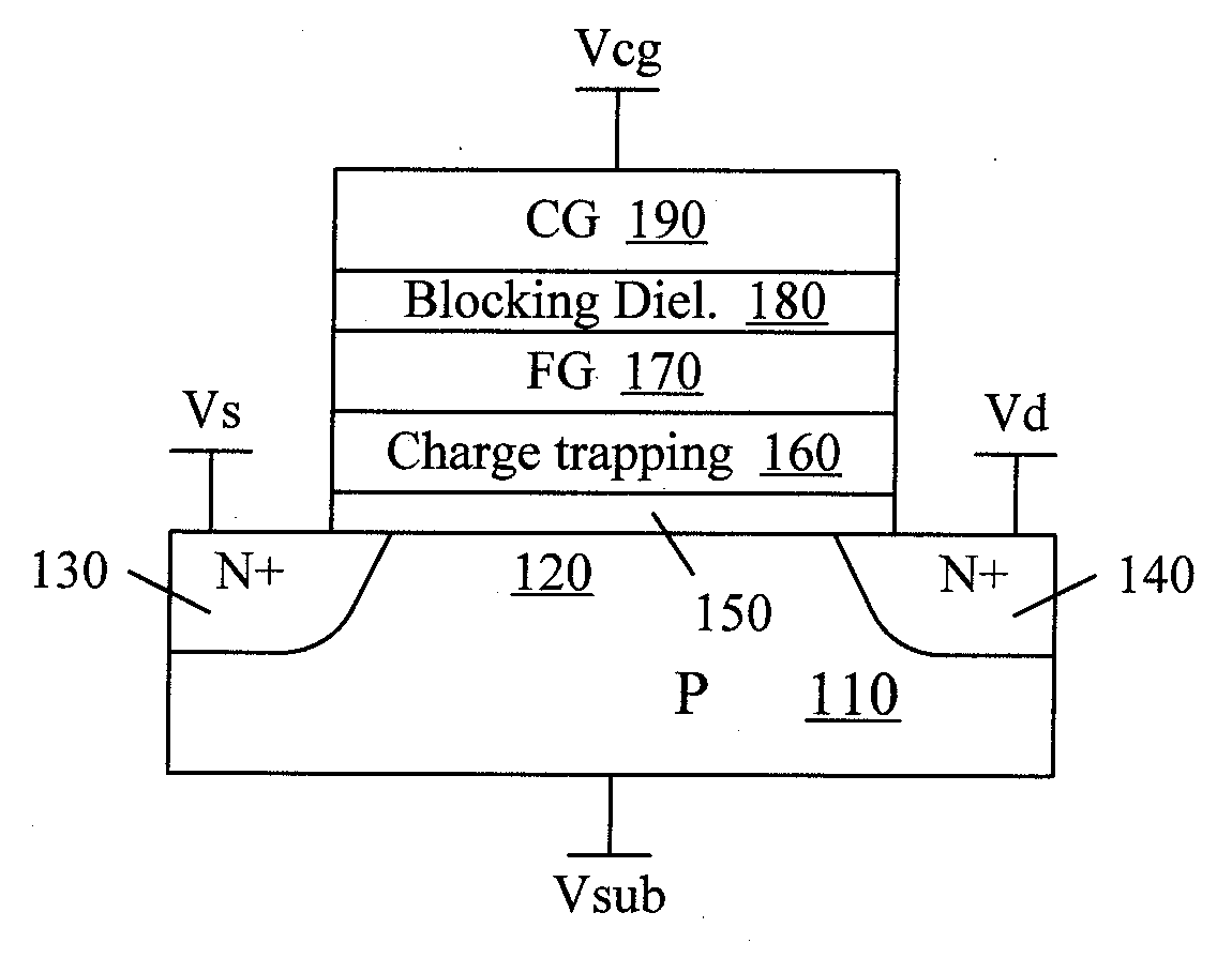
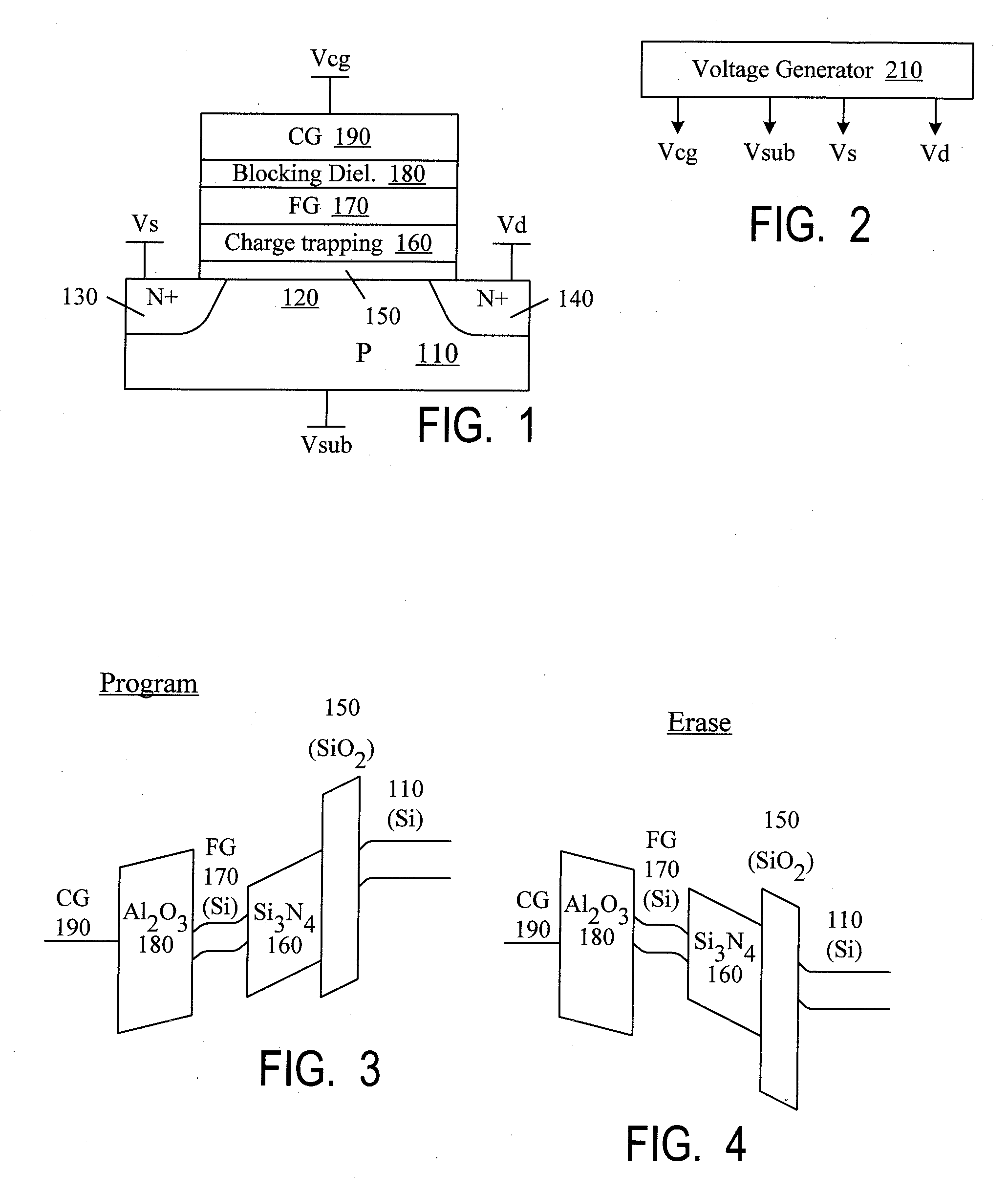
[0013]FIG. 1 shows a vertical cross section of a nonvolatile memory cell according to some embodiments of the present invention. The cell's active area is a semiconductor region which is part of a semiconductor substrate 110. Substrate 110 can be monocrystalline silicon or some other suitable material. The active area includes a P-type channel region 120 and N-type source / drain regions 130, 140 (the P and N conductivity types can be reversed). For ease of reference, the region 130 will be called “source”, and the region 140 will be called “drain”. In fact, in some embodiments each of regions 130, 140 can act as a source or a drain in the same cell in different modes of operation.

[0014]Tunnel dielectric 150 is formed directly on the active area over the c...


PUM


Abstract

A nonvolatile memory cell stores at least 50% of the charge in a dielectric, charge-trapping layer (160) and at least 20% of the charge in a floating gate (170). The floating gate is at most 20 nm thick.

Description

BACKGROUND OF THE INVENTION[0001]The present invention relates to nonvolatile memories which store electric charge to define the memory state.[0002]A nonvolatile memory may have a charge storage element for storing charge to define the memory state. The charge storage element can be conductive (a floating gate) or dielectric (a charge trapping element). In either case, the charge storage capacity of the charge storage element must be sufficiently large to allow fast, reliable reading of the memory state. Floating gates are typically made of doped polysilicon, and the polysilicon thickness of 100 nm or higher is not unusual to provide sufficient charge storage capacity. This large thickness is an impediment to scaling the memory area because the thickness-to-width ratio of the floating gate becomes high when the width is reduced, and the memory becomes more difficult to fabricate. In addition, the tunnel dielectric has to be fairly thick (typically above 6 nm for silicon dioxide) to ...

Claims


Application Information

Patent Timeline
IPC IPC(8): H01L29/788H01L21/336
CPCH01L21/28273H01L21/28282H01L29/792H01L29/7885H01L29/7883H01L29/40114H01L29/40117
Inventor DONG, ZHONGCHEN, CHILIANGCHEN, CHING-HWA
Owner PROMOS TECH PTE LTD
Why Eureka
Try Eureka