Plasma Display Panel and Method for Manufacturing Same

Inactive Publication Date: 2009-04-16
PANASONIC CORP
View PDF2 Cites 13 Cited by
  • Summary
  • Abstract
  • Description
  • Claims
  • Application Information

AI Technical Summary

Benefits of technology

[0032]In accordance with the present invention, the protective film has a structure in which grain-state crystals are aggregated, and on the surface of the protective film, an area occupied by voids among the crystals is set in a range of from 0% or more to less than 10%, with respect to the area of the protective film; therefore, it becomes possible to obtain a protective film that is superior in the sputtering resistant property. Consequently, great effects are achieved such that a PDP that is superior in image quality with high precision, an

Problems solved by technology

Moreover, in response to an increase in the number of scanning lines in an attempt to provide high precision devices, it is necessary to narrow the pulse width of an address pulse to be applied to the address electrodes so as to carry out a high speed driving operation; however, in a high precision PDP actually manufactured, due to a discharge delay phenomenon in which discharging takes place with a considerable delay from the rise of an applied pulse, the possibility of completing a discharge within an applied pulse width becomes lower, causing a phenomenon such as a fail

Method used


Image

  • Plasma Display Panel and Method for Manufacturing Same
  • Plasma Display Panel and Method for Manufacturing Same
  • Plasma Display Panel and Method for Manufacturing Same

Examples


embodiments

[0050]Referring to FIGS. 1A to 8, the following description will discuss one embodiment of the present invention.

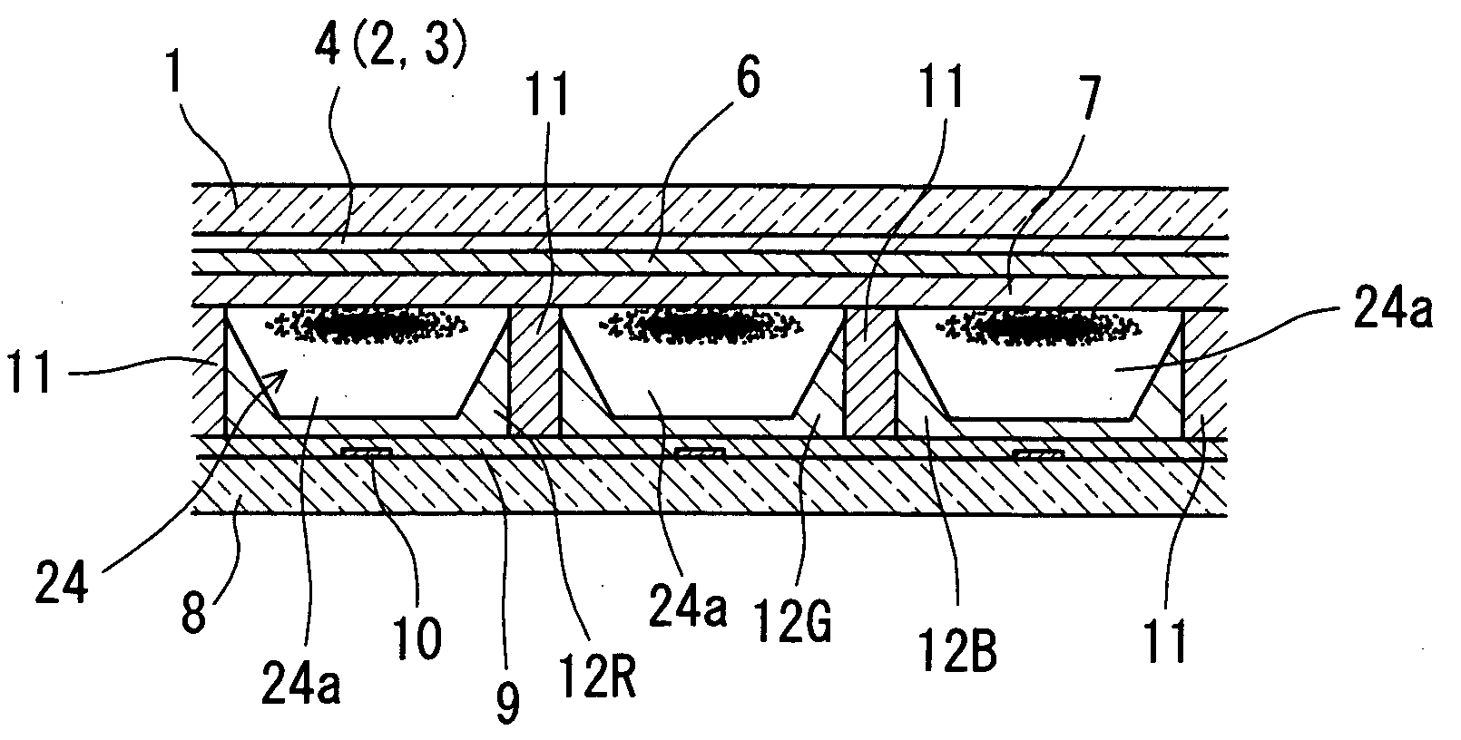
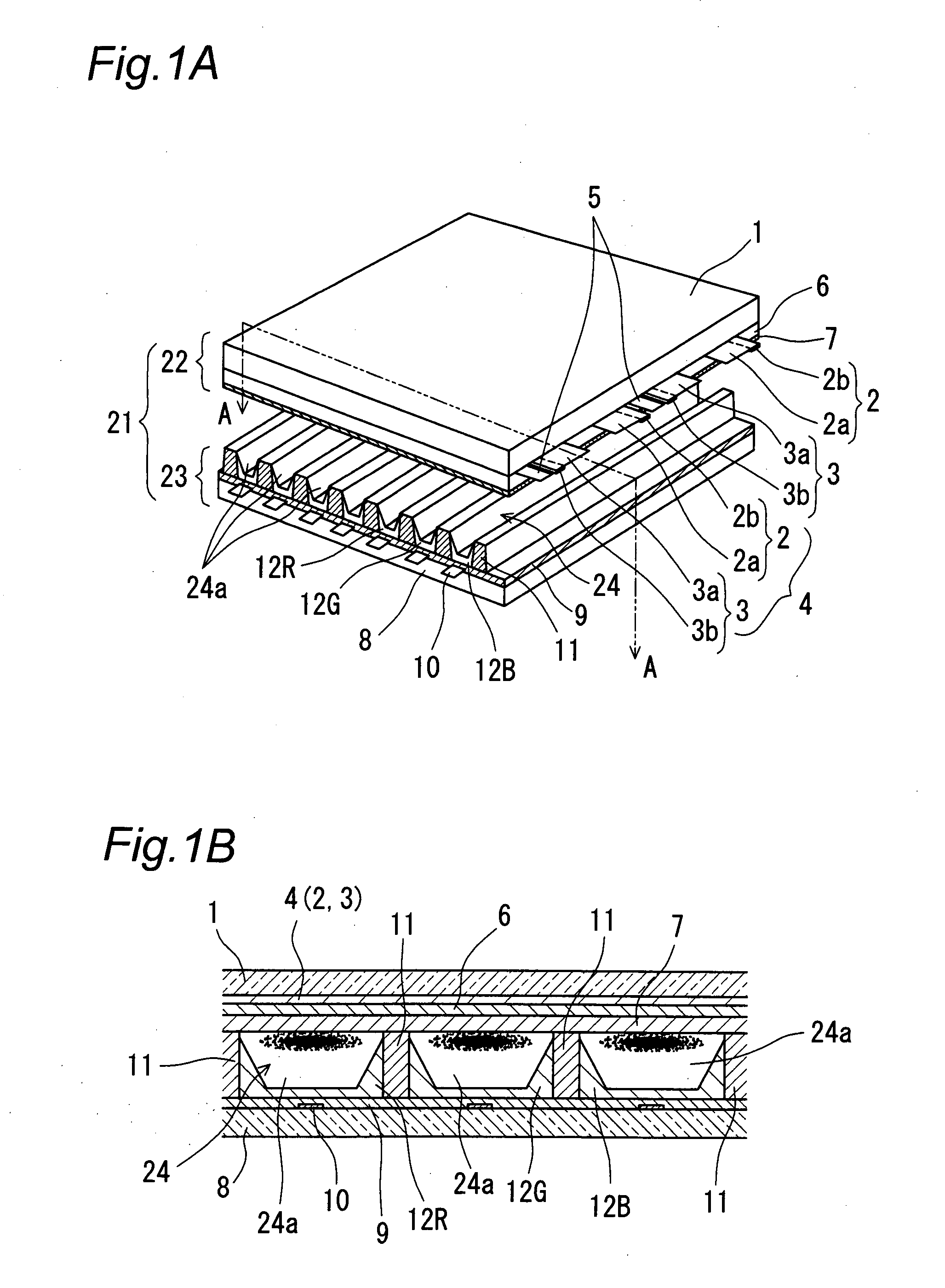
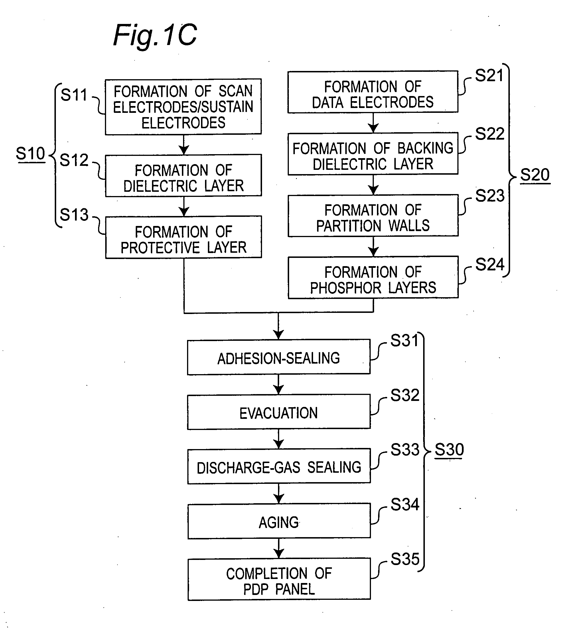
[0051]FIG. 1A is an exploded perspective view that shows an enlarged structure of one portion of an AC-type PDP in accordance with the embodiment of the present invention, FIG. 1B is a cross-sectional view that shows an AA portion of FIG. 1A in an enlarged manner, and FIG. 1C is a flow chart of manufacturing processes that schematically explains a manufacturing method of the AC-type PDP in the embodiment of the present invention. Here, the structure of the general AC-type PDP has already been explained by reference to FIGS. 9A and 9B as the prior art, and although the AC-type PDP in accordance with the embodiment of the present invention has a structure similar to the structure in which line electrodes and column electrodes are arranged orthogonally on a front glass substrate 1 and a back glass substrate 8 made of glass, respectively so that an intersection between two li...


PUM

PropertyMeasurementUnit
Fractionaaaaaaaaaa
Fractionaaaaaaaaaa
Densityaaaaaaaaaa

Abstract

A PDP, which has a plurality of display electrodes formed therein, and is provided with a front plate in which the display electrodes are covered with a first dielectric layer and a protective film and a back plate having a plurality of address electrodes that are formed in a direction orthogonal to the display electrode, and covered with a second dielectric layer (backing dielectric layer, is designed so that the protective film has a structure in which grain-state crystals are aggregated and a grain size of the crystals is large, with a void between adjacent crystals being formed with a small size.

Description

TECHNICAL FIELD[0001]The present invention relates to a plasma display panel (hereinafter, referred to as PDP) which has become widely applied as a flat-panel-type display apparatus (referred to also as flat panel display) for use in a large-size television as well as in a public display for advertisement, information, and the like, and also concerns a method for manufacturing such a plasma display panel. In particular, the present invention relates to a plasma display panel with a protective film, which is used at a low output and capable of maintaining superior display quality even after long time operations, and a manufacturing method for such a plasma display panel.BACKGROUND ART[0002]In recent years, the PDP, used as a large-size flat panel display, in which ultraviolet rays, generated by the discharge of rare gas, excite phosphors to emit light to realize an image / video image display, has been developed to achieve such a large-size product as to have a diagonal length of 1 m o...

Claims


Application Information

Patent Timeline
IPC IPC(8): H01J17/49H01J9/20C23C14/34H01J17/04
CPCH01J9/02H01J11/40H01J11/12
Inventor YAMASHITA, HIDEKIOKUMA, TAKAFUMIHAYATA, HIROSHITAKII, YOSHIMASANAKAUE, HIROKAZUKIMURA, TADASHITERAUCHI, MASAHARU
Owner PANASONIC CORP
Why Eureka
Try Eureka