Substrate dividing method

a substrate and dividing technology, applied in the direction of printed circuits, printed circuit components, printed circuit manufacturing, etc., can solve the problems of reducing strength, cracking or cracking in the corner portions of the corner portions, and damage to the semiconductor or silicon chip, so as to improve the strength of individual substrate pieces and prevent the cracking of the corner portions of individual substrate pieces

Inactive Publication Date: 2009-04-16
SHINKO ELECTRIC IND CO LTD
View PDF4 Cites 39 Cited by
  • Summary
  • Abstract
  • Description
  • Claims
  • Application Information

AI Technical Summary

Benefits of technology

[0024]According to the substrate dividing method of the present invention, the chamfering through holes are formed in the intersecting positions of the dividing lines on the substrate, and then the substrate is divided into individual pieces along the dividing lines. Therefore, respective corner portions of the individual pieces of the substrate are chamfered and thus, the strength of individual pieces of the substrate can be improved and individual pieces of the substrate can be handled easily.
[0025]Further, the through holes for forming the chamfering are formed on the substrate in advance. Therefore, in cutting or dividing the substrate, the corner portions of individual pieces of the substrate are prevented from chipping or opening cracks in the corner portions.

Problems solved by technology

As a result, such a problem comes up that the corner portions are chipped off or cracks open in the corner portions.
In addition, such a problem existed that, in conveying the semiconductor chip or the silicon chip or joining the semiconductor chip or the silicon chip to the mounting substrate, the semiconductor chip or the silicon chip is damaged.
In particular, if a thickness of the semiconductor chip or the silicon chip is thin, there is a problem that strength is lowered and the semiconductor chip or the silicon chip easily breaks in handling.
The problem such that the corner portions of the chip are chipped or the chipping occurs in the cutting positions when individual semiconductor chips or silicon chips are formed from the semiconductor wafer or the silicon substrate is not limited to the case where the semiconductor wafer or the silicon substrate is handled.
Of course, such problem may arise similarly in the step of dicing a substrate such as a glass substrate, a ceramic substrate, or the like into substrates in unit of individual piece.

Method used


Image

  • Substrate dividing method
  • Substrate dividing method
  • Substrate dividing method

Examples


Embodiment Construction

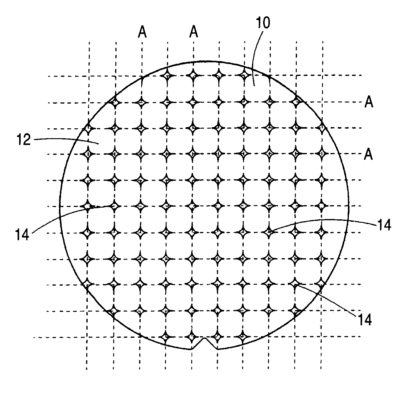
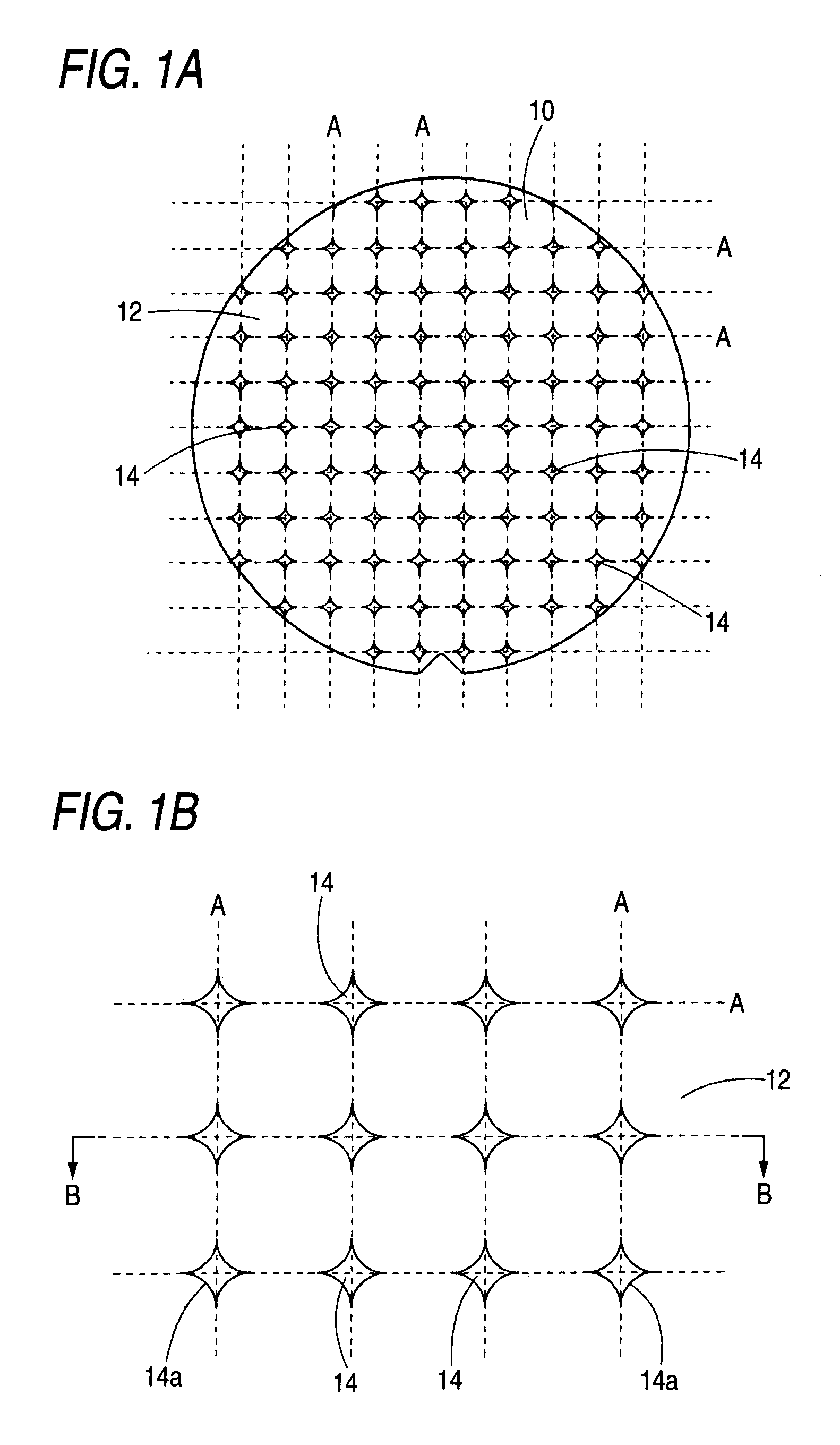
[0035]FIGS. 1A and 1B show a step of forming divide silicon chips from a silicon substrate, as an example of a substrate dividing method according to the present invention.

[0036]FIGS. 1A and 1B show states that chamfering patterns 14 from which a surface of a silicon substrate 10 is exposed are formed by coating a resist 12 on the surface of the silicon substrate 10 and then exposing and developing the resist 12. The chamfering patterns 14 are aligned lengthwise and crosswise at a predetermined interval and are provided at positions which correspond to intersection points where dividing lines A for dividing the silicon substrate 10 into individual pieces are intersected mutually. (The dividing lines may be virtual lines.)

[0037]The chamfering patterns 14 are shown in an enlarged manner in FIG. 1B. The chamfering pattern 14 is provided so as to chamfer respective corner portions of individual divide silicon chips 20 when the silicon substrate 10 is divided into individual pieces. The ...


PUM


Abstract

A method of dividing a substrate 10 into individual pieces by setting dividing lines A used to dividing the substrate 10 into individual pieces at a predetermined interval in a vertical direction and a horizontal direction and then dividing the substrate 10 along the dividing lines A, includes a step of forming chamfering patterns 14 to form through holes, which are used to chamfer corner portions of individual pieces of the substrate, in respective intersection points between the dividing lines on the substrate, a step of forming chamfering through holes by etching the substrate 10, and a step of obtaining the individual pieces of the substrate by separating the substrate in the vertical direction and the horizontal direction along the dividing lines A respectively.

Description

BACKGROUND OF THE INVENTION[0001]1. Field of the Invention[0002]The present invention relates to a substrate dividing method of dividing a substrate such as a semiconductor wafer, a silicon substrate, or the like into individual pieces.[0003]2. Description of Related Art[0004]In the step of forming a semiconductor chip from a semiconductor wafer, the step of forming a substrate (silicon chip) for an interposer from a silicon substrate, and the like, the work of forming individual semiconductor chips or silicon chips by dicing the semiconductor wafer or the silicon substrate must be done.[0005]FIG. 8 shows an example in which a semiconductor wafer 5 is diced to obtain the semiconductor chips as individual pieces from the semiconductor wafer 5. The semiconductor wafer 5 is separated into individual semiconductor chips 8 by pasting a dicing tape on the semiconductor wafer 5 and then moving dicing blades along the dicing lines 6 to cut the semiconductor wafer 5.[0006]As the method of di...

Claims


Application Information

Patent Timeline
Patent Type & Authority Applications(United States)
IPC IPC(8): H01L21/302
CPCH01L21/78H01L21/3083H05K1/0306H05K3/0029H05K3/0052H05K3/0097H05K2201/09027H05K2201/09036H05K2201/09063H05K2201/0909H05K2203/302H01L21/302
Inventor TAGUCHI, YUICHISHIRAISHI, AKINORISUNOHARA, MASAHIROMURAYAMA, KEISAKAGUCHI, HIDEAKIHIGASHI, MITSUTOSHI
Owner SHINKO ELECTRIC IND CO LTD
Why Eureka
Try Eureka