
Space minimized flash drive

a space-minimized, flash drive technology, applied in the direction of sustainable manufacturing/processing, coupling device connection, final product manufacturing, etc., can solve the problems of increasing costs, complex chip design, empty footprints on printed circuit boards that are not utilized, etc., to achieve the effect of reducing the length of the flash drive and increasing manufacturing costs

Inactive Publication Date: 2009-04-16
WALTON ADVANCED ENG INC
View PDF10 Cites 15 Cited by
  • Summary
  • Abstract
  • Description
  • Claims
  • Application Information

AI Technical Summary

Benefits of technology

The present invention provides a space-minimized flash drive that reduces the length of the flash drive without increasing manufacturing costs. The flash drive has a printed circuit board with contact fingers, a first memory device, and a controller. The printed circuit board has a component section and an insertion section extending into the USB connector. The contact fingers are on the insertion section and the first memory device is on the component section. The controller is on the bottom surface of the insertion section. The flash drive has the advantage of saving space and reducing manufacturing costs. The memory devices can be on both top and bottom surfaces of the printed circuit board. The manufacturing process is easy and the component section and insertion section can be formed at the same time. The printed circuit board strengths can be increased to avoid damage to the controller. The passive components are disposed inside the flash drive to reduce both the component footprint and the empty space footprint.

Problems solved by technology

In an existing structure, the dimensions of the controllers or passive components are smaller than those of the memory devices, leaving some empty footprints on the printed circuit board that are not utilized.
Although RDL is fabricated during the IC fabrication of memory devices in wafer form, the chip design is complicated and increases costs.
When two different memory devices in chip forms are needed in a conventional USB flash drive, one with RDL and the other without RDL, increasing the complexity of chip management.
Moreover, once the design of RDL is finalized, then the dimensions of controllers and passive components in chip forms are also fixed, and thus multiple sources of controllers and passive components cannot easily be found at lower prices, leading to a reduced selection of controllers and passive components in the market and higher manufacturing costs and difficulties.

Method used


Image

  • Space minimized flash drive
  • Space minimized flash drive
  • Space minimized flash drive

Examples


first embodiment

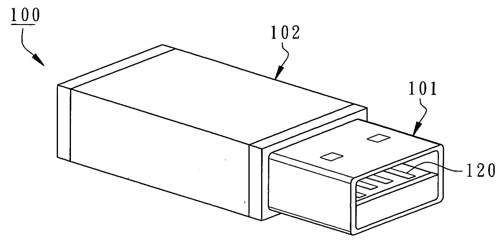
[0022]According to the present invention, a space-minimized flash drive 100 has a USB connector 101 and a body 102 where the USB connector 101 is a relatively square metal case disposed at the front end of the body 102. More specifically, the USB connector 101 is a standard A-type USB connector which can be inserted into a USB socket of a primary system, such as a personal computer, where data can be accessed and stored through the USB connector 101.

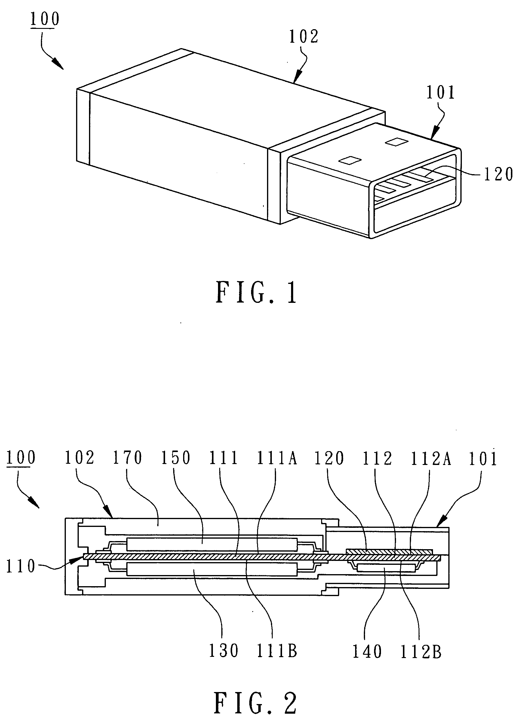
[0023]As shown in FIG. 2, the flash drive 100 primarily comprises a printed circuit board 110, a plurality of contact fingers 120, a first memory device 130, and a controller 140.

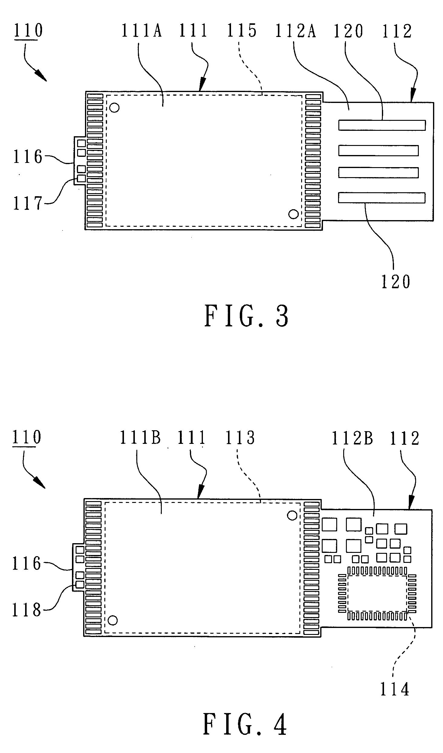
[0024]As shown in FIG. 2, the printed circuit board 110 has a component section 111 located inside the body 102 and an insertion section 112 extending into and located inside the USB connector 101. Typically the printed circuit board 110 is a high-density double-sided multi-layer printed circuit board with internal traces as electrical transferring media. The co...

second embodiment

[0034]In the present invention, as shown in FIG. 6, another space-minimized flash drive 200 is shown having a USB connector 201 and a body 202. The flash drive 200 primarily comprises a printed circuit board 210, a plurality of contact fingers 220, a first memory device 230, a controller 240, and a second memory device 250, in which the printed circuit board 210 has a component section 211 located inside the body 202 and an insertion section 212 extended into the USB connector 201. The contact fingers 220 are disposed on the top surface 212A of the insertion section 212.

[0035]As shown in FIG. 6, in the present embodiment, a first memory device 230 and a second memory device 250 are flash memories and are respectively disposed on the bottom surface 211B and the corresponding top surface 211A of the component section 211 of the printed circuit board 210 by way of COB processes and are electrically connected to the printed circuit board through wire bonding. Additionally, the controlle...


PUM


Abstract

A space-minimized flash drive has a USB connector and a body, where the flash drive comprises a printed circuit board, a plurality of contact fingers, one or more memory devices, and a controller. The printed circuit board has a component section located inside the body and an insertion section extending into and located inside the USB connector. The memory device is disposed on the component section. The contact fingers are disposed on the top surface of the insertion section. The controller is disposed on the bottom surface of the insertion section located inside the USB connector. The footprint occupied by the controller and the corresponding empty footprint are saved to effectively reduce the length of the flash drive to miniaturize flash drives without interfering with the electrical connections of the contact fingers when plugging in the flash drive.

Description

FIELD OF THE INVENTION[0001]The present invention relates to a miniature semiconductor storage device, and more particularly to a space-minimized flash drive.BACKGROUND OF THE INVENTION[0002]Flash drives normally have USB connectors to plug into USB sockets of electronic devices for data storage and access. USB stands for “Universal Serial Bus” and is an international connector standard. USB provides multiple advantages for end users, such as ease of use, expandability, and high data transfer rates, and therefore the USB standard has been widely implemented in various electronic devices, computers, IA, and 3C consumer products and has become a necessity in everyday lives.[0003]The USB connector is located at the front end of a flash drive and is formed by a rectangular metal case with a plastic insulator, where four USB contact fingers are disposed on the surface of the plastic insulator. The plastic insulator is formed from a solid resin material on a rigid substrate, such as white...

Claims


Application Information

Patent Timeline
Patent Type & Authority Applications(United States)
IPC IPC(8): H01R13/648
CPCH01R13/7175H01R31/065H05K1/117H05K1/181H05K2201/10159H05K2203/1572H01L2224/16225H01L2224/73265H01L2224/48227H01L2224/32225H01L2924/00012H01L24/73Y02P70/50
Inventor CHENG, CHIH-CHIENLIN, TSE-MING
Owner WALTON ADVANCED ENG INC
Learn More