
Eureka
For R&D, Eureka makes reading and utilizing patents & technical documents easy.
Eureka AIR
Designed for self-driven R&D workflows. Generate viable solutions, solve complex R&D challenges, empower your innovation with AI.

Eureka Materials
Designed for material experts only. Revolutionize your material R&D, from search, analyze, to developing new materials.

TechResearch
Generate reliable direction feasibility study reports for your R&D in just a few steps.

TechSeek
Discover and master advanced knowledge NOW. Basics, ideas, possibilities, all at once.

TechMind
As an expert in R&D Theories, TechMind can generates customized viable solutions instantly.

TechRisk
Analyze your overall solution with one click, know your potential R&D risks in advance.

TechMonitor
Get weekly tech updates, stay abreast of the latest tech innovations and key insights.
Plasma processing apparatus and method for detecting status of said apparatus
- Summary
- Abstract
- Description
- Claims
- Application Information
AI Technical Summary
Benefits of technology
Problems solved by technology
Method used
Image

Examples
embodiment 1
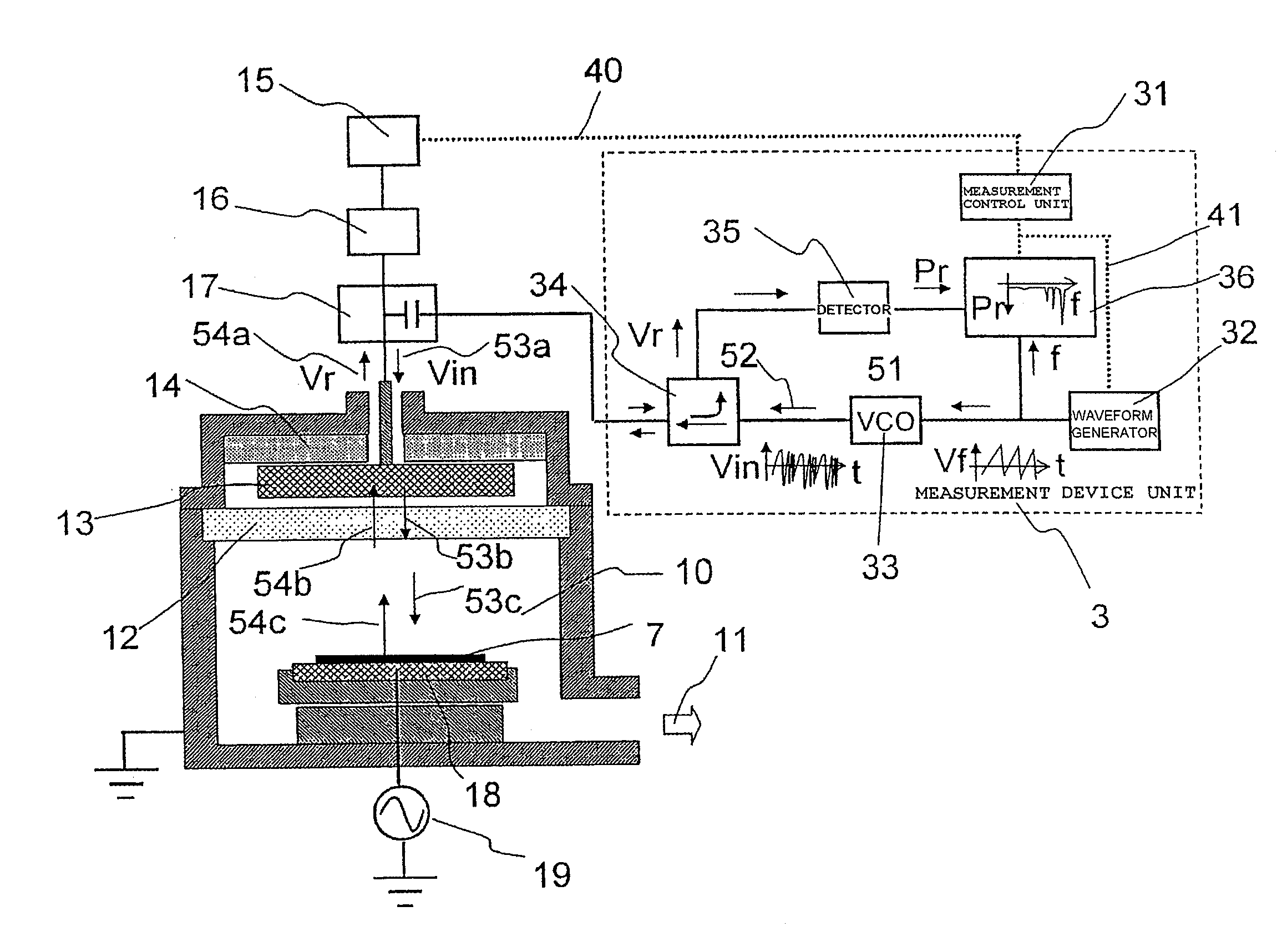
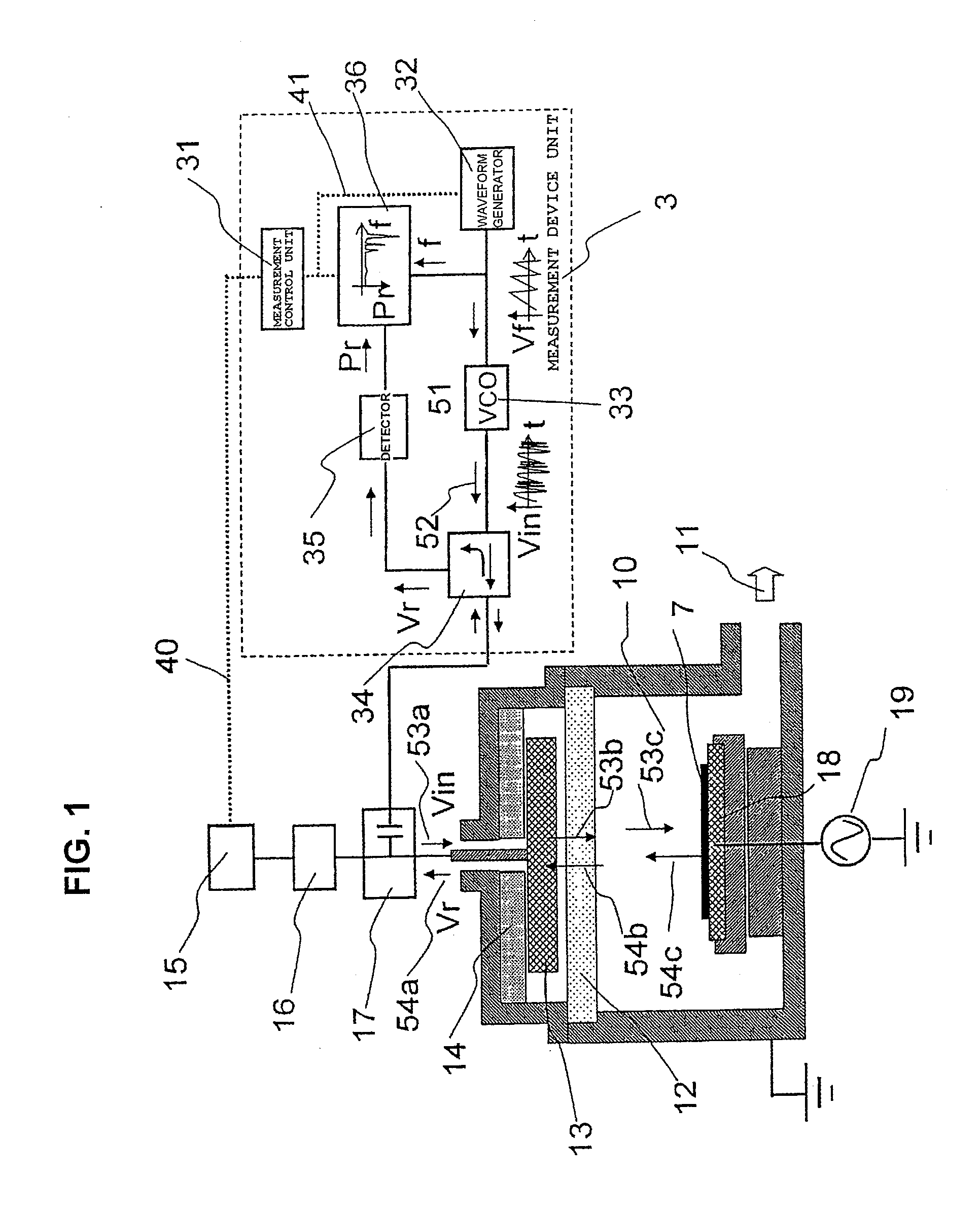
[0041]With reference to FIG. 1, the outline of the arrangement of a plasma processing apparatus according to a first embodiment of the present invention will be described. The plasma processing apparatus of the present embodiment is a parallel plate plasma processing apparatus using microwaves or high frequency waves.
[0042]The plasma processing apparatus includes a vacuum processing chamber 10 formed within a casing (vacuum reactor), a vacuum means 11, a vacuum window 12, a high frequency electrode (high frequency transmission unit) 13, an insulating support member 14, a processing apparatus control unit 15, a plasma-generating high frequency power supply 16, a high frequency matching unit 17, an electrostatic chuck (attraction electrode) 18, an RF bias high frequency power supply 19 and a measurement device unit (frequency spectrum measuring means) 3.
[0043]A substrate to be processed (wafer) 7 is attracted and held on the electrostatic chuck 18. A connector not shown can be arrange...
embodiment 2
[0072]The outline of the arrangement of a plasma processing apparatus according to a second embodiment of the present invention will be described with reference to FIG. 8. The plasma processing apparatus in the present embodiment is an inductively-coupled plasma processing apparatus.
[0073]According to the embodiment of FIG. 8, the inductively-coupled plasma processing apparatus includes a vacuum processing chamber 10 formed within a casing (vacuum reactor), a processing apparatus control unit 15, a plasma-generating high frequency power supply 16, a high frequency matching unit 17, an electrostatic chuck (attraction electrode as high frequency transmission means) 18, an RF bias high frequency power supply 19, a vacuum means not shown, an insulating vacuum window 20, a high frequency coil 21, a high frequency matching unit 22, and a measurement device unit 3.
[0074]A substrate to be processed (wafer) 7 is attracted and held on the electrostatic chuck 18. A connector not shown can be a...
PUM
| Property | Measurement | Unit |
|---|---|---|
| Power | aaaaa | aaaaa |
| Sensitivity | aaaaa | aaaaa |
| Frequency | aaaaa | aaaaa |
Abstract
Description
Claims
Application Information
 - R&D Engineer
- R&D Manager
- IP Professional
- Industry Leading Data Capabilities
- Powerful AI technology
- Patent DNA Extraction
Browse by: Latest US Patents, China's latest patents, Technical Efficacy Thesaurus, Application Domain, Technology Topic, Popular Technical Reports.
© 2024 PatSnap. All rights reserved.Legal|Privacy policy|Modern Slavery Act Transparency Statement|Sitemap|About US| Contact US: help@patsnap.com