Semiconductor device and method for manufacturing the same

a semiconductor device and manufacturing method technology, applied in the direction of semiconductor devices, semiconductor/solid-state device details, electrical apparatus, etc., can solve the problems of increasing the cost of manufacture, prolonging the manufacturing period of the semiconductor device, etc., to achieve the effect of improving the manufacturing yield of the semiconductor device and easy formation of through-hole electrodes

Active Publication Date: 2009-04-30
LONGITUDE LICENSING LTD
View PDF8 Cites 87 Cited by
  • Summary
  • Abstract
  • Description
  • Claims
  • Application Information

AI Technical Summary

Benefits of technology

[0074]Accordingly, it is possible to provide a semiconductor device which makes it possible to easily form a through-hole electrode therein and improve the manufacturing yield of the semiconductor device,

Problems solved by technology

Consequently, the above-described method causes not only the prolongation of the manufacturing period of the semiconductor device but also an increase in the cost of manufacture.
This results in the problem of variation caused when creating openings by etching silicon substrate 151 and interlayer insulating film 153.
Also in this regard, the above-described method causes the prolongation of the manufacturing period of the semiconductor device and an increase in the cost of manufacture.

Method used


Image

  • Semiconductor device and method for manufacturing the same
  • Semiconductor device and method for manufacturing the same
  • Semiconductor device and method for manufacturing the same

Examples


first embodiment

2-1 First Embodiment

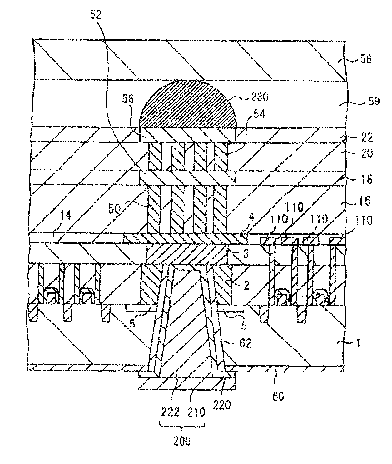
[0151]A semiconductor device of the first embodiment comprises:

[0152]a fourth insulating layer, a semiconductor silicon layer, a first insulating layer, a second insulating layer and a third insulating layer formed in order;

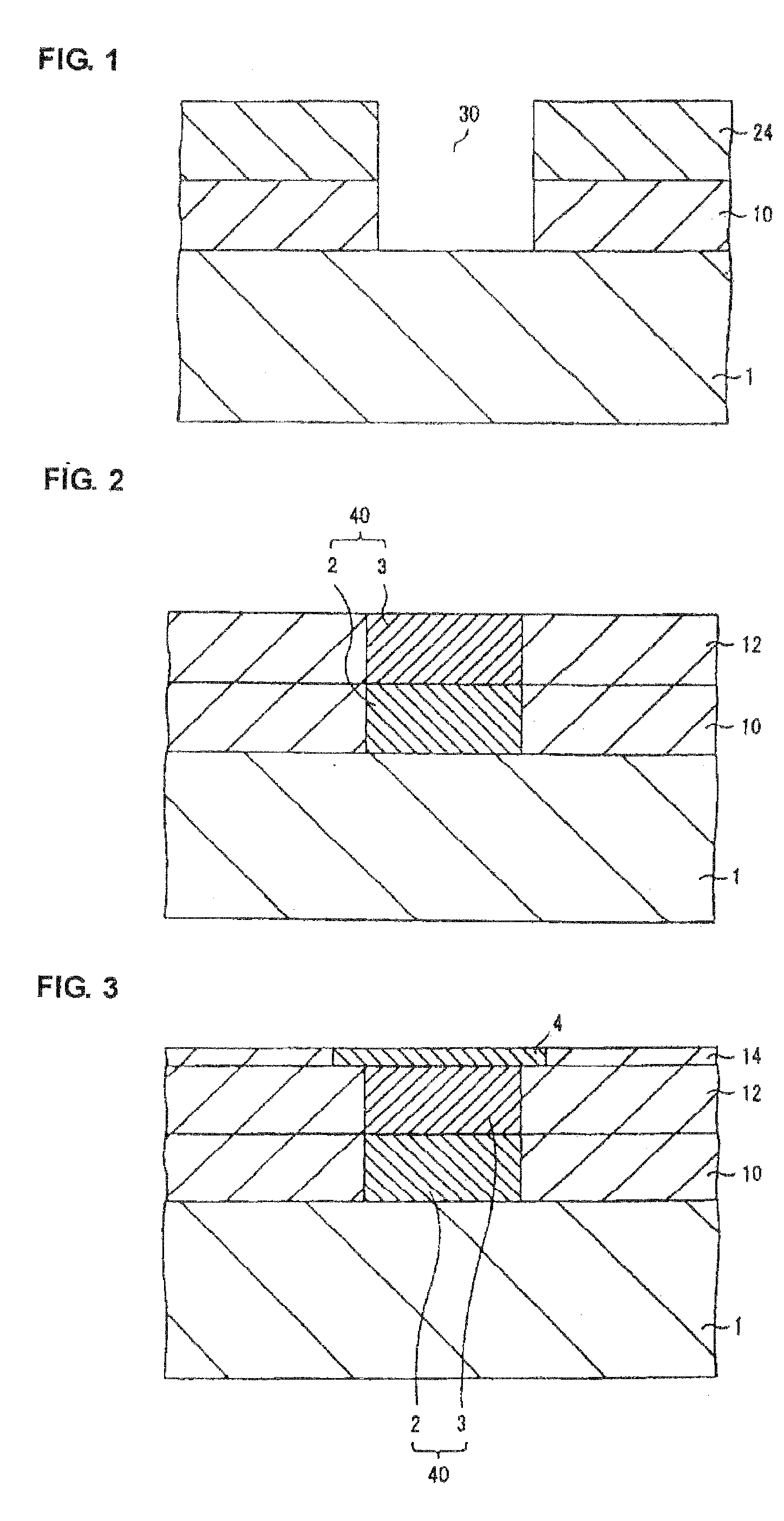
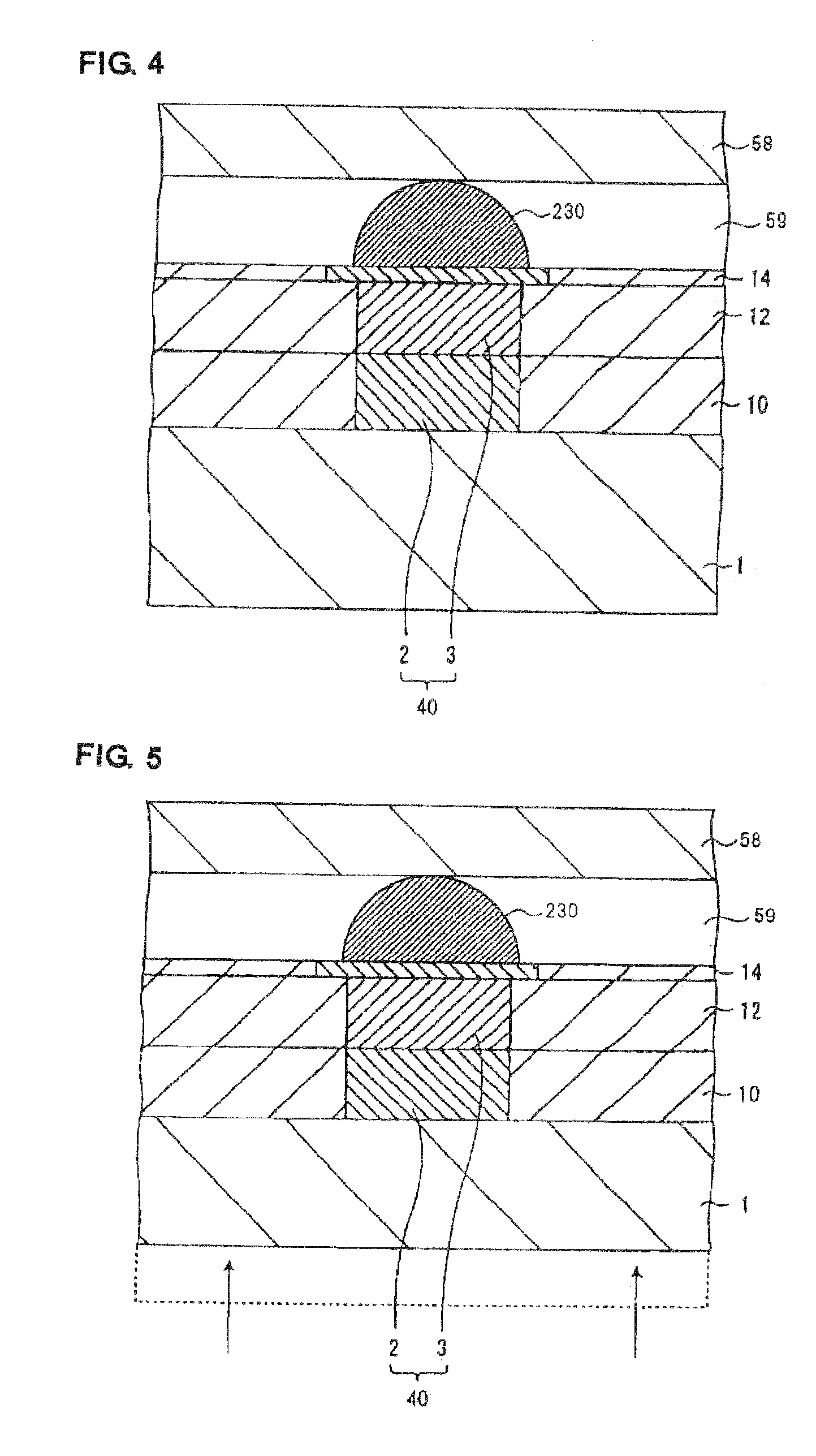
[0153]a first contact pad penetrating through the first insulating layer in the thickness direction of the first insulating layer and made of conductive polysilicon;

[0154]a second contact pad and an interconnect layer formed so as to respectively penetrate through positions corresponding to the first contact pad within the second and the third insulating layers in the thickness directions of the second and the third insulating layers;

[0155]a through-hole electrode formed so as to penetrate through at least the fourth insulating layer, the semiconductor silicon layer and the first contact pad to reach to the second contact pad;

[0156]a fifth insulating layer formed at least between the through-hole electrode and the semiconductor silicon layer; ...

second embodiment

2-2 Second Embodiment

[0158]A semiconductor device of the second embodiment comprises:

[0159]a fourth insulating layer, a semiconductor silicon layer, a first insulating layer, a second insulating layer and a third insulating layer formed in order;

[0160]a first contact pad penetrating through the first insulating layer in the thickness direction of the first insulating layer and made of conductive polysilicon;

[0161]a second contact pad and an interconnect layer formed so as to respectively penetrate through positions corresponding to the first contact pad within the second and the third insulating layers in the thickness directions of the second and the third insulating layers;

[0162]a through-hole electrode formed so as to penetrate through at least the fourth insulating layer, the semiconductor silicon layer and the first contact pad to reach to the second contact pad; and

[0163]a cylindrical insulator surrounding the through-hole electrode and penetrating through the semiconductor si...

second exemplary embodiment

[0258]The present exemplary embodiment is directed at manufacturing a semiconductor device basically using the manufacturing method of the second embodiment. FIG. 22 is a schematic cross-sectional view of a substantial part used to explain a step of manufacturing a semiconductor device of the second embodiment. As shown in FIG. 22, cylindrical electrode / substrate-separating hole 240 is first formed from the front surface side of semiconductor silicon layer 1.

[0259]That is, a photoresist layer is first formed over the front surface side of semiconductor silicon layer 1 (not illustrated). An opening pattern is formed in this photoresist layer by a publicly-known lithography method. Using this opening pattern as a mask, cylindrical electrode / substrate-separating hole 240 is formed so as to surround a region of semiconductor silicon layer 1 in which a through-hole electrode is to be formed. Cylindrical electrode / substrate-separating hole 240 can be formed by, for example, anisotropic et...


PUM


Abstract

A first insulating layer including a first contact pad made of conductive polysilicon and a second insulating layer including a second contact pad are formed over a semiconductor silicon layer. After this, a via hole for a through-hole electrode is formed until the via hole penetrates through at least the semiconductor silicon layer and the first contact pad and reaches to the second contact pad.

Description

[0001]This application is based upon and claims the benefit of priority from Japanese Patent Application No 2007-280338, filed on Oct. 29, 2007, the disclosure of which is incorporated herein in its entirety by reference.BACKGROUND OF THE INVENTION[0002]1. Field of the Invention[0003]The present invention relates to a semiconductor device comprising a through-hole electrode and a method for manufacturing the semiconductor device.[0004]2. Description of the Related Art[0005]Conventionally, the mainstream of semiconductor device configuration has been that a single semiconductor device is equipped with a single semiconductor silicon layer. In recent years, however, there have been proposed such semiconductor device configuration in which a single semiconductor device is equipped with a plurality of semiconductor silicon layers. More specifically, it is possible to enhance the capabilities of a semiconductor device, including the processing speed, while reducing the size and weight of ...

Claims


Application Information

Patent Timeline
Patent Type & Authority Applications(United States)
IPC IPC(8): H01L23/48H01L21/44
CPCH01L21/6835H01L21/76898H01L2924/1306H01L2224/13111H01L2924/01047H01L2924/01033H01L2924/01023H01L2924/01006H01L2924/30105H01L2924/19041H01L2924/14H01L2924/04953H01L23/481H01L24/12H01L2221/68372H01L2224/13025H01L2224/13099H01L2224/2518H01L2924/01002H01L2924/01005H01L2924/01013H01L2924/01015H01L2924/01022H01L2924/01029H01L2924/01073H01L2924/01074H01L2924/01078H01L2924/01079H01L2924/04941H01L2924/00014H01L2924/01028H01L2924/00H01L2924/12036H01L2224/05085H01L2224/05009H01L2224/0557H01L2224/05568H01L2224/05001H01L2224/05124H01L2224/05147H01L2224/05166H01L2224/05184H01L2224/05025H01L24/05H01L24/03H01L24/06H01L24/13
Inventor UCHIYAMA, SHIRO
Owner LONGITUDE LICENSING LTD
Why Eureka
Try Eureka