Structure for capacitive balancing of integrated relative humidity sensor

Active Publication Date: 2009-04-30
HONEYWELL INT INC
8 Cites 7 Cited by

AI-Extracted Technical Summary

Problems solved by technology

It has been found, however, that elements utilized as resistive components suffer from the disadvantage that there is an inherent dissipation effect caused by the dissipation of heat due to the current flow in the elements necessary to make a resistance measurement.
The result includes erroneous readings, among other problems.
In addition, there can also be inaccuracy incurred at high relative humidity values where high water content causes problems due to excessive stress and the resulting mechanical shifts in the components of th...

Method used

[0037]A humidity sensitive dielectric layer can be formed on the second insulator layer and the pair of capacitor plates, wherein a relative permittivity of the humidity sensitive layer varies in accordance with a humidity such that a pair of series capacitance additionally varies in accordance with the humidity to thereby provide an increased accurate measurement of the humidity. Additionally, a porous electrically conductive plate can be configured on the humidity sensitive dielectric layer, wherein t...

Benefits of technology

[0015]It is, therefore, one aspect of the present invention to provide for improved sensor methods and systems.
[0016]It is another aspect of the present invention to provide for an improved structure for capacitive balancing of relative humidity sensors in the presence of water and/or moisture condensation.
[0017]The aforementioned aspects and other objectives and advantages can now be achieved as described herein. An improved relative humidity sensor for more accurate measurement of humidity in the presence of water condensation is disclosed. The relative humidity sensor generally includes a pair of electrodes with a gap-interposed therebetween to form series sensing capacitors on a silicon substrate with a silicon oxide film configured on a surface. A moisture-sensitive structure can be provided so as to cover the pair of capacitor plates with a silicon nitride film interposed therebetween. A P-well and a P-plus layer can be added to the perimeter of the substrate to create a path ...

Abstract

An improved relative humidity sensor apparatus that provides a more accurate measurement of humidity in the presence of water condensation. A series capacitive sensor includes a thin porous platinum top plate, a humidity sensitive polyimide dielectric, and two metal bottom plates on a semiconductor substrate. The two capacitors can be wired in series such that the metal bottom plates form independent, electrically driven connections. The thin top layer can form a top plate. Changes in humidity affect the humidity sensitive dielectric thereby causing changes in the capacitive value. A P-well layer and a P-plus layer can be added at the perimeter of the substrate to create a path for a parasitic capacitance caused by water condensation to connect to one or more connection nodes, thereby preventing erroneous measurements of humidity in the presence of water condensation.

Application Domain

Technology Topic

Image

  • Structure for capacitive balancing of integrated relative humidity sensor
  • Structure for capacitive balancing of integrated relative humidity sensor
  • Structure for capacitive balancing of integrated relative humidity sensor

Examples

  • Experimental program(1)

Example

[0023]The particular values and configurations discussed in these non-limiting examples can be varied and are cited merely to illustrate at least one embodiment and are not intended to limit the scope thereof.
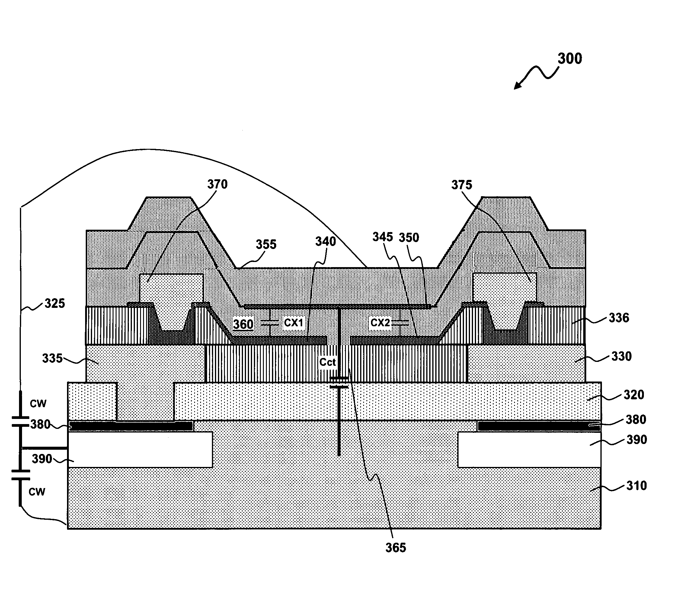
[0024]Referring to FIG. 3, a cut-away side view of an improved relative humidity sensor apparatus 300 is illustrated, in accordance with a preferred embodiment. It should be understood that there are other integrated components of the sensor that are not depicted in the figure. The humidity sensor apparatus 300 depicted in FIG. 3 can be used for humidity control in an air conditioner or to detect humidity for weather observation purposes. It is understood, however, that a wide variety of other applications for humidity sensor apparatus 300 can also be implemented, depending upon design goals and considerations. As depicted in FIG. 3, an N-type silicon substrate 310 can be employed as a semiconductor substrate 310. A silicon oxide film 320 can be formed on the semiconductor substrate 310 as a first insulation film. First and second electrodes 330 and 335 are configured on an identical plane of the silicon oxide film 320 so as to oppose each other with a gap 365 interposed between them.
[0025]A material capable of being utilized in a normal semiconductor fabrication facility can be employed to form the first and second electrodes 330 and 335. Such material can be, for example, Al, Ti, Au, Cu, poly-Si, and the like. In one particular embodiment, a silicon nitride film 336 can be formed on first insulation film 320 and around the electrodes 330 and 335 as a second insulation film. It can be appreciated, however, that in other embodiments, materials other than silicon nitride may be utilized to implement film 336. The silicon nitride film 336 can be formed by plasma CVD method or the like, so as to have the same thickness over the whole area on the semiconductor substrate 310.
[0026]As shown in FIG. 3, the pair of electrodes 330 and 335 can be equipped with a first electrical contact 370 and a second electrical contact 375 through which the electrodes 330 and 335 are connected to a signal processing circuit (not shown in FIG. 3) for detecting the variation of the sensing capacitance between the pair of electrodes 330 and 335, respectively. Furthermore, according to such an embodiment, the capacitance type humidity sensor apparatus 300 can be formed on the semiconductor substrate 310, and thus the signal processing circuit for detecting the variation of the capacitance type humidity sensor apparatus 300 can be formed on the principal surface of the semiconductor substrate 310.
[0027]A sensing medium 360 having a permittivity that changes according to humidity can be formed on capacitor plates 340, 345, and silicon nitride layer 336. Porous platinum top plate 350 through which water is allowed to permeate can be formed so as to cover the humidity sensing medium 360. When water infiltrates into the humidity sensing medium 360, the dielectric constant of the humidity sensing medium 360 is varied in accordance with the amount of water.
[0028]As a result, the series sensing capacitors as indicated by CX1 and CX2 are constructed by the pair of plates 340, 345, and the top porous plate 350 with the humidity sensing medium 360 as a part of the dielectric material. Humidity can be detected on the basis of the sensing capacitance between the pair of electrodes 330 and 335, because the amount of water contained in the humidity sensing medium 360 corresponds to the ambient humidity around the capacitance type humidity sensor apparatus 300.
[0029]As described above, the variation of the capacitance between the pair of electrodes 330 and 335 in accordance with the humidity variation of the humidity sensing medium 360 can be increased with increasing relative humidity.
[0030]A P-well layer 390 (i.e., an example of a second semiconductor substrate) can be formed on the surface of the silicon semiconductor substrate 310. A P-plus layer 380 can be diffused above the P-well layer. The P-well layer 390 and P-plus layer 380 can be fabricated by implanting appropriate dopants below the buried oxide layer 320. The layers can also be fabricated utilizing standard silicon wafer processing techniques commonly used in silicon wafer fabrication.
[0031]The P-well layer 390 and the P-plus layer 380 create a path 325 for the parasitic capacitance CW caused by water condensation to connect to one node of the sensing capacitor CX1 (i.e., the sensing capacitor CX1 of the sensing medium 360). The relative humidity sensing capacitor CX1 and CX2 can be fabricated utilizing standard silicon wafer processing techniques commonly used to configure existing relative humidity sensors. Formation of the P-well layer 390 and the P-plus layer 380 can be accomplished by taking advantage of photo-mask changes in the wafer fabrication process flow.
[0032]A hygroscopic macro molecule organic material can be employed as the moisture sensing medium 360. Specifically, a polyimide or butyric acetyl cellulose or the like can be employed. In such an embodiment, the sensing medium 360 can be composed of a polyimide. When molecular water is absorbed in the film 360, the permittivity of the film 360 changes according to the amount of absorbed water molecules, since water molecules have a high permittivity, which thereby causes a change in capacitance between the detection electrodes 330 and 335. An area where the moisture-sensitive film 360 is located on the semiconductor substrate 310 constitutes a humidity-sensing portion 360. Namely, ambient humidity can be detected via the humidity-sensing portion 360 based on the capacitance formed between the detection electrodes 330 and 335.
[0033]The total capacitance between the pair of electrodes 330 and 335 in response to changes in the surrounding humidity can be expressed in the form of equation (3) as follows:
CTotal=(CX1*CX2)/(CX1+CX2+Cct)   (3)
[0034]The total capacitance value due to the presence of water condensation is given by equation (4):
CTotal=((CX1+CW)*CX2)/((CX1+CW)+CX2+Cct))   (4)
[0035]As demonstrated by equation (4), the total capacitance value CTotal in presence of water condensation on the sensor increases since the parasitic capacitance CW path is re-directed to the sensing capacitor CX1, which provides a more accurate measurement of humidity.
[0036]In general, the methodology for forming the sensor apparatus 300 can be implemented as follows. A semiconductor substrate and a first insulator layer can be formed on the semiconductor substrate in association with a second insulator layer formed on the first insulator layer. A P-plus layer and a P-well can be then be formed on a perimeter of the semiconductor substrate wherein the P-plus layer and the P-well layer create a path for a parasitic capacitance caused by water condensation to connect to at least one node of a sensing capacitor. A pair of contacts can be associated with capacitor plates formed on the first insulator layer in association with a pair of capacitor plates formed on the second insulator layer, wherein the pair of capacitor plates are isolated from one another with a space formed therein.
[0037]A humidity sensitive dielectric layer can be formed on the second insulator layer and the pair of capacitor plates, wherein a relative permittivity of the humidity sensitive layer varies in accordance with a humidity such that a pair of series capacitance additionally varies in accordance with the humidity to thereby provide an increased accurate measurement of the humidity. Additionally, a porous electrically conductive plate can be configured on the humidity sensitive dielectric layer, wherein the porous electrically conductive plate includes a common top plate with respect to the pair of capacitive plates. A protective layer can be formed on the porous electrically conductive plate, wherein the protective layer protects the common top plate and the humidity sensitive layer. The first insulator layer can constitute silicon oxide and the second insulator layer can be silicon nitride. The P-plus layer and the P-well layer can be fabricated utilizing a standard silicon wafer processing technique.
[0038]The disclosed device can be utilized to sense the relative humidity in the ambient environment around the sensor. During operation, a relative humidity level can be sensed and then the sensor generates a voltage output proportional to the relative humidity. This voltage can then be used by other circuits to implement functions such as, for example, relative humidity control, enthalpy control for building HVAC, weather sensing instruments, process controls for drying, process controls for batch or any continuous production where relative humidity is a parameter that controls the output of a process or is related to some process variable to be controlled, length or end of cycle in drying applications, and other applications.
[0039]It will be appreciated that variations of the above-disclosed and other features and functions, or alternatives thereof, may be desirably combined into many other different systems or applications. Also that various presently unforeseen or unanticipated alternatives, modifications, variations or improvements therein may be subsequently made by those skilled in the art which are also intended to be encompassed by the following claims.

PUM

no PUM

Description & Claims & Application Information

We can also present the details of the Description, Claims and Application information to help users get a comprehensive understanding of the technical details of the patent, such as background art, summary of invention, brief description of drawings, description of embodiments, and other original content. On the other hand, users can also determine the specific scope of protection of the technology through the list of claims; as well as understand the changes in the life cycle of the technology with the presentation of the patent timeline. Login to view more.

Similar technology patents

Photo frame structure

Owner:GREAT SUN TECH CORP

Seating device with a foldable table

InactiveUS20070216201A1Improved support structureImprove structureDismountable chairsFoldable chairsEngineering
Owner:CRAZY CREEK PRODS

Classification and recommendation of technical efficacy words

  • Improve structure
  • Accurately measure

Implantable sensor method and system

ActiveUS20090030297A1Accurately measureBioelectric signal measurementSurgical needlesElectrode arrayIntegrated circuit
Owner:MEDTRONIC MIMIMED INC

System and Method for Illumination and Fixation with Ophthalmic Diagnostic Instruments

ActiveUS20080284979A1Accurately measureLess noiseRefractometersSkiascopesOptical pathDiagnostic instrument
Owner:AMO DEVMENT

Body-worn monitor for measuring respiratory rate

ActiveUS20110257489A1Accurately measureReduce occurrenceInertial sensorsCatheterExercise frequencyRespiratory rate
Owner:SOTERA WIRELESS
Why Eureka
Try Eureka