Self-Triggering CMOS Image Sensor

a self-triggering, image sensor technology, applied in the direction of color television details, television system details, television systems, etc., can solve the problems of increasing the exposure of patients without generating a useful image, non-zero dark current, and inconvenient us

Active Publication Date: 2009-04-30
BAE SYST IMAGING SOLUTIONS
View PDF7 Cites 21 Cited by
  • Summary
  • Abstract
  • Description
  • Claims
  • Application Information

AI Technical Summary

Problems solved by technology

Hence, conventional systems lack a synchronization system that can be used by the solid state image sensor.
Any exposure that occurs prior to the image sensor entering the image accumulation mode is wasted, and hence, increases the exposure of the patient without generating a useful image.
Unfortunately, the photodiodes in the imaging array generate a non-zero dark current which would be accumulating during the period between the reset and the start of the exposure.
The accumulated dark current would result in an unacceptable background that could only be overcome by increasing the exposure.
Unfortunately, this strategy requires that the existing millions of x-ray machines al

Method used


Image

  • Self-Triggering CMOS Image Sensor
  • Self-Triggering CMOS Image Sensor
  • Self-Triggering CMOS Image Sensor

Examples


Embodiment Construction

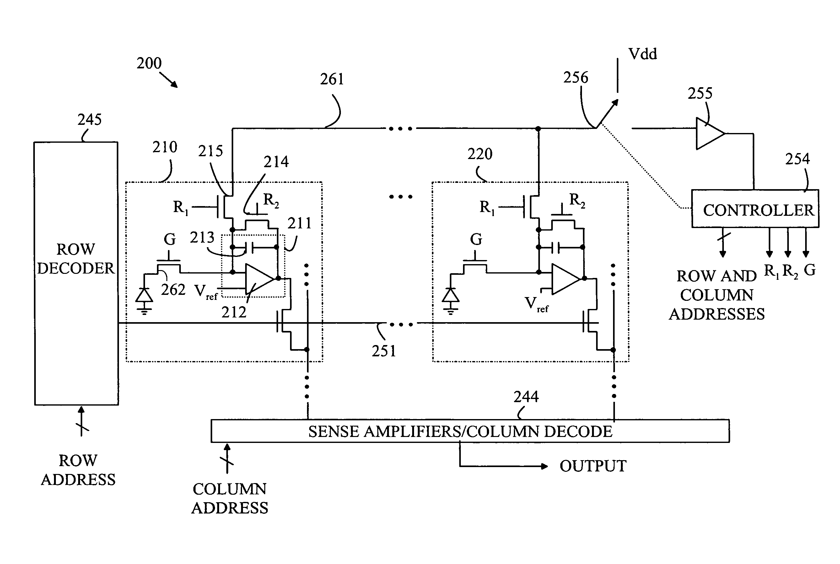
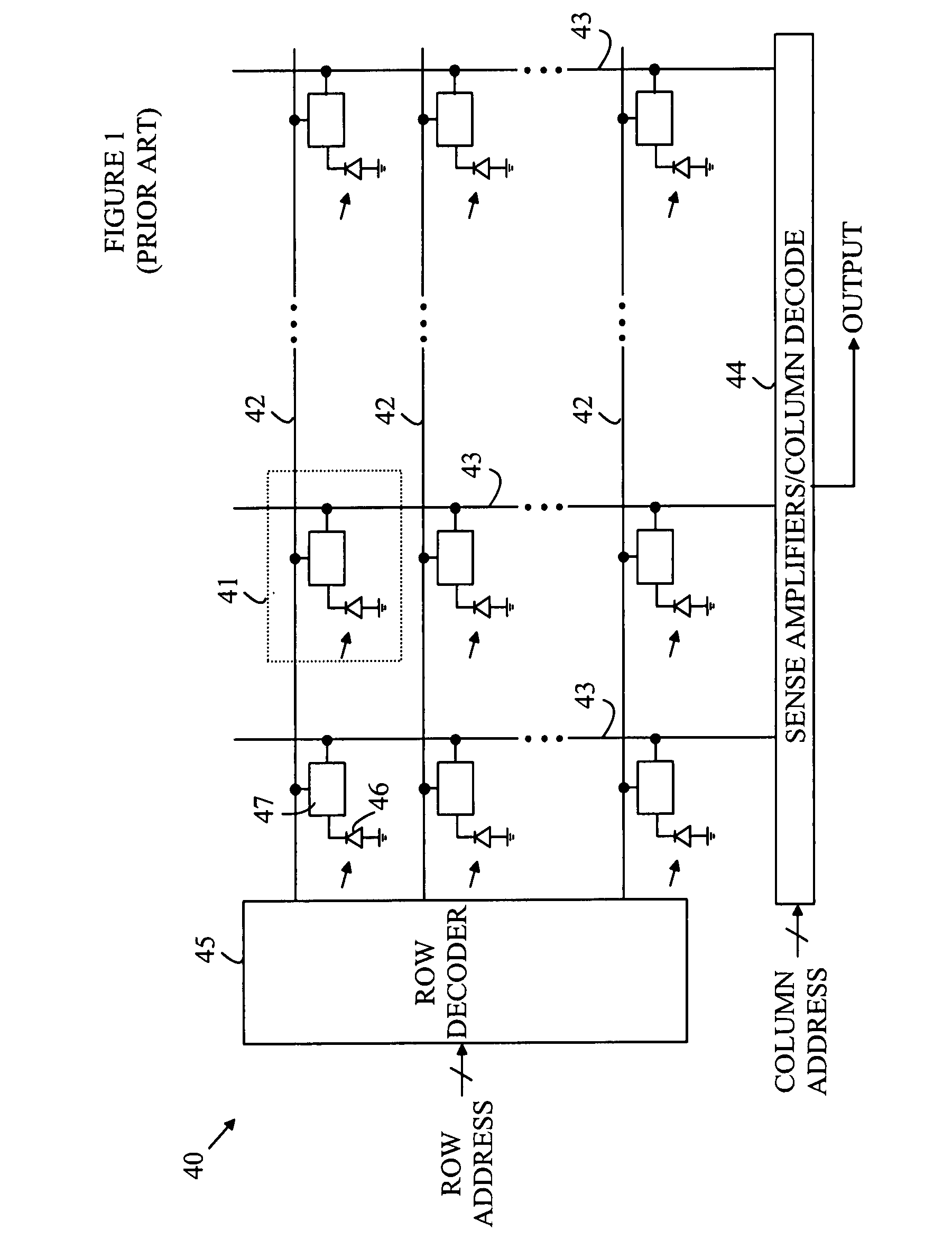
[0018]The manner in which the present invention provides its advantages can be more easily understood with reference to FIG. 1, which is a schematic drawing of a prior art CMOS imaging array. Imaging array 40 is constructed from a rectangular array of pixel sensors 41. Each pixel sensor includes a photodiode 46 and an interface circuit 47. The details of the interface circuit depend on the particular pixel design. However, all of the pixel sensors include a gate that is connected to a row line 42 that is used to connect that pixel sensor to a bit line 43. The specific row that is enabled at any time is determined by a row address that is input to a row decoder 45. The row select lines are a parallel array of conductors that run horizontally in the metal layers over the substrate in which the photodiodes and interface circuitry are constructed.

[0019]The various bit lines terminate in a column processing circuit 44 that typically includes sense amplifiers and column decoders. The bit ...


PUM


Abstract

An image sensor and method for using the image sensor to capture an image are disclosed. The image sensor includes an imaging array, a first block amplifier and a controller. A first plurality of pixels in the imaging array includes pixels having a photodiode connected to a first node by a gate transistor, a reset transistor connected between the first node and a reset node, a pixel amplifier having an input connected to the first node and an output, and an output gate for connecting the pixel amplifier output to an output bus. The sensor has a monitoring mode and an image capture mode. In the monitoring mode the reset node is connected to the first block amplifier whose output is monitored and used to trigger the image capture mode when the output exceeds a predetermined threshold.

Description

BACKGROUND OF THE INVENTION[0001]Solid state image sensors have replaced conventional film for capturing images in cameras. The image sensor typically includes a two-dimensional array of pixels. Each pixel includes a photodiode that records the light received at one point in the scene that is being recorded. To capture an image, each pixel is reset prior to the scene being imaged onto the sensor. After a predetermined exposure time, the image is blocked from measuring any further light and the charge stored by each photodiode is readout to provide an image of the scene.[0002]In a conventional camera, the exposure is controlled by a shutter that is triggered in response to the user pushing a button. The image sensor is reset just before the shutter opens and is readout at a predetermined time after the shutter closes. These operations are synchronized to the user pushing the button.[0003]In some applications, the imaging array must determine when the exposure begins without the aid o...

Claims


Application Information

Patent Timeline
IPC IPC(8): H04N5/335H04N5/343H04N5/3745H04N5/376
CPCH04N3/155H04N5/343H04N5/335H04N5/32H04N25/42
Inventor LIU, XINQIAODO, HUNG
Owner BAE SYST IMAGING SOLUTIONS
Why Eureka
Try Eureka