Method for programming non-volatile memory

a non-volatile memory and programming method technology, applied in static storage, digital storage, instruments, etc., can solve the problems of affecting the performance of the memory, the process of programming, and the reading and erasing of memory cells, so as to shorten the programming time of the memory, increase programming efficiency, and save power consumption

Inactive Publication Date: 2009-04-30
POWERCHIP SEMICON CORP
View PDF4 Cites 9 Cited by
  • Summary
  • Abstract
  • Description
  • Claims
  • Application Information

AI Technical Summary

Benefits of technology

[0015]In terms of the method for programming non-volatile memory of the present invention, since a substrate hot carrier effect is adopted to inject carriers into the charge storage layer for programming operations, thus, the required program operation voltage is low, which are helpful to save power consumption, increase programming efficiency, shorten the programming time of the memory and enhance the reliability of the devices. Moreover, by using an appropriate forward bias voltage applied to the fir

Problems solved by technology

However, for an NAND type array structure, the procedures of programming, reading and erasing memory cells thereof are more complicate.
As a result, the junction breakdown voltage of the tunneling oxide layer is accordingly reduced, which makes the tunneling oxide layer u

Method used


Image

  • Method for programming non-volatile memory
  • Method for programming non-volatile memory
  • Method for programming non-volatile memory

Examples


Embodiment Construction

[0023]Reference will now be made in detail to the present preferred embodiments of the invention, examples of which are illustrated in the accompanying drawings. Wherever possible, the same reference numbers are used in the drawings and the description to refer to the same or like parts.

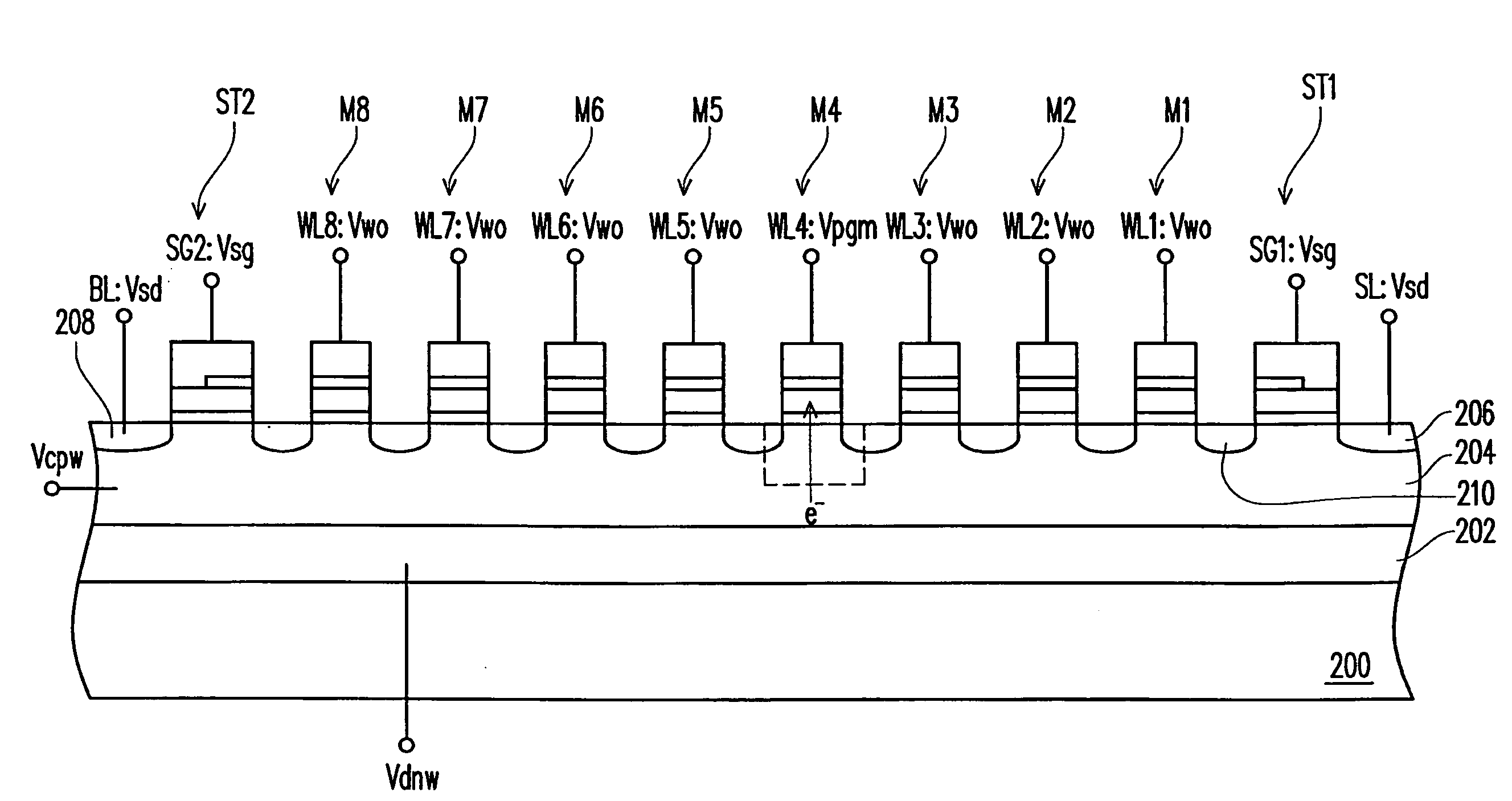
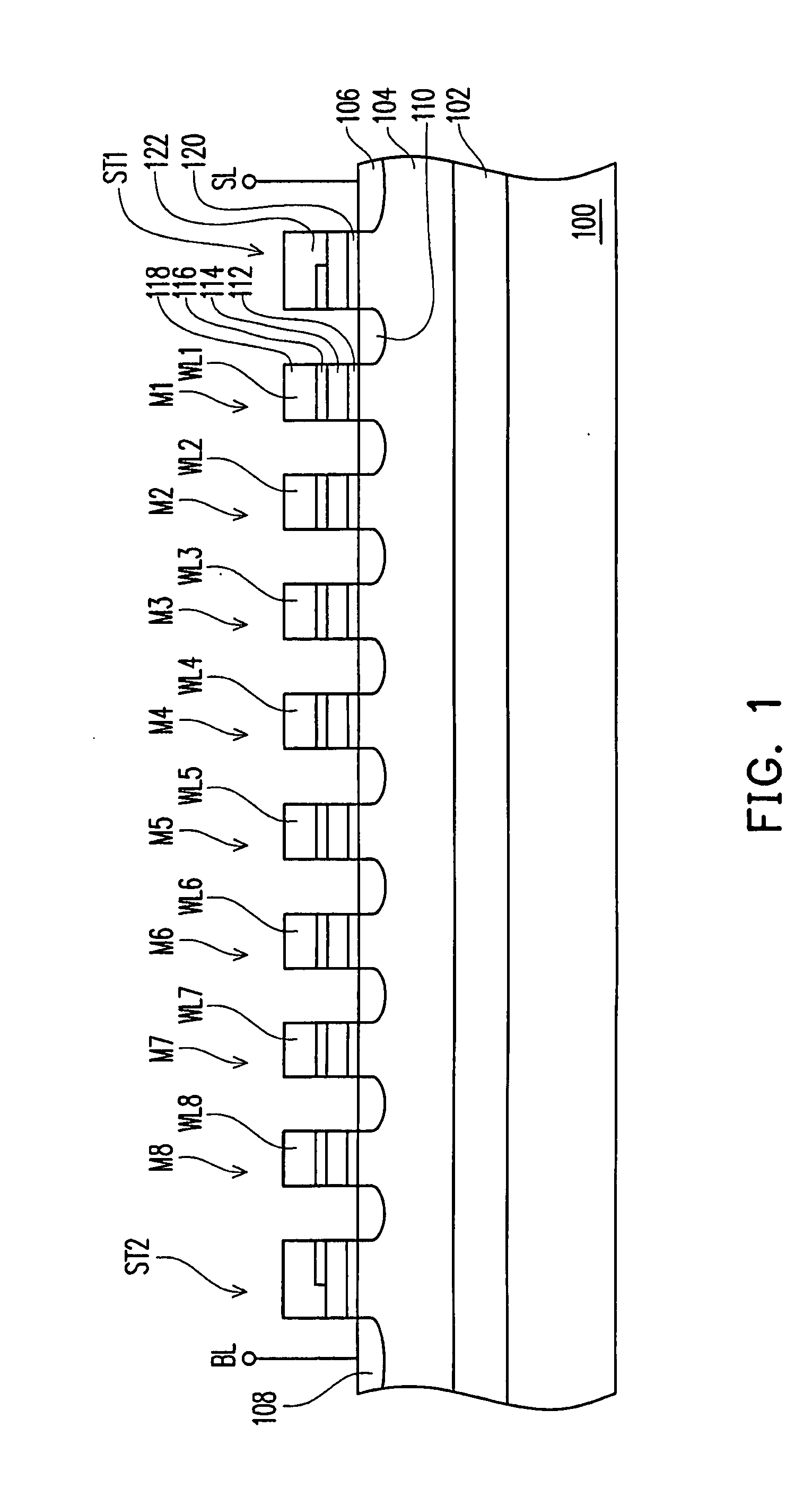
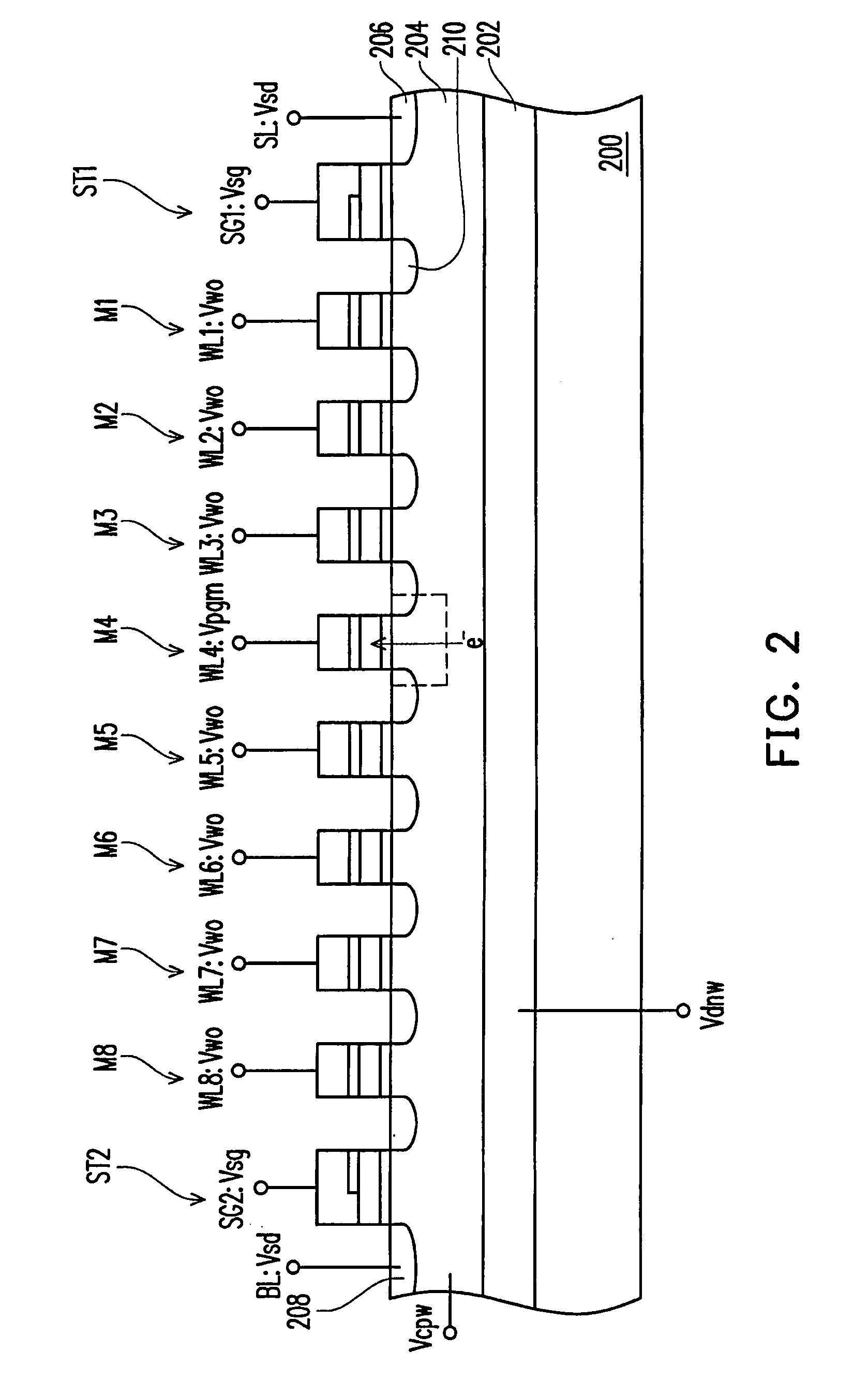
[0024]FIG. 1 is a schematic cross-sectional drawing of an NAND type non-volatile memory.

[0025]Referring to FIG. 1, an NAND type non-volatile memory includes, for example, a first conductive type substrate 100, a second conductive type well region 102, a first conductive type well region 104, a second conductive type source region 106, a second conductive type drain region 108, a first select transistor ST1, a plurality of memory cells M1-M8 and a second select transistor ST2, wherein if the first conductive type is P-type, the second conductive type is N-type; if the first conductive type is N-type, the second conductive type is P-type.

[0026]The first conductive type substrate 100 is, for example, a ...


PUM


Abstract

A method for programming non-volatile memory utilizes substrate hot carrier effect to conduct programming operations. A forward bias voltage is applied between an N-type well region and a P-type well region so as to inject electrons in the N-type well region into the P-type well region. After that, the electrons are accelerated by a depletion region established by a voltage applied to a source region and a drain region, and a vertical electrical field established between a control gate and the P-type well region further forces the electrons to be injected into a charge storage layer. Since the present invention adopts the substrate hot carrier effect to inject carriers into the charge storage layer, the required program operation voltage is low, which benefits to save power consumption and enhance the reliability of the device.

Description

BACKGROUND OF THE INVENTION[0001]1. Field of the Invention[0002]The present invention generally relates to an operation method of non-volatile memory, and more particularly, to a method for programming NAND type non-volatile memory.[0003]2. Description of Related Art[0004]Among various kinds of memory products, the non-volatile memory is a kind of memory characterized by the advantages that it allows multiple data storing, reading or erasing operations. The data stored in the non-volatile memory will be retained even if the power applied to the device is cut off. The non-volatile memory has become a widely adopted memory device in personal computers and electronic equipments.[0005]A typical non-volatile memory device usually has a stacked gate structure which includes a floating gate and a control gate both made of doped polysilicon. The floating gate is located between the control gate and a substrate. The floating gate is in floating status without wiring any circuit. The control ...

Claims


Application Information

Patent Timeline
IPC IPC(8): G11C11/34
CPCG11C16/10G11C16/0483
Inventor HUANG, CHEN-HAOHUNG, CHIH-WEICHEN, CHIH-YUAN
Owner POWERCHIP SEMICON CORP
Why Eureka
Try Eureka