Semiconductor memory device having biderectional buffer

a memory device and semiconductor chip technology, applied in the direction of digital storage, electric digital data processing, instruments, etc., can solve the problems of increasing the area required for the wirings of the semiconductor chip, affecting the speed of data transmission, so as to reduce the chip area required for wiring and consumption current, and the effect of high-speed data transmission tim

Active Publication Date: 2009-04-30
LONGITUDE LICENSING LTD
View PDF6 Cites 2 Cited by
  • Summary
  • Abstract
  • Description
  • Claims
  • Application Information

AI Technical Summary

Benefits of technology

[0010]The present invention seeks to solve the above problem and provides a semiconductor memory device in which high-speed data transfer time is ensured by shortening wiring length of a data bus. Thereby, a plurality of individual data buses connected to different areas of a memory cell array are provided in any arrangement, and data transmitted bidirectionally between a common data bus and the individual data buses can be selectively buffered, in order to reduce both chip area required for wiring and consumption current.

Problems solved by technology

Wiring capacitance and resistance of the data bus increase due to the increase in the wiring length of the data bus, thereby causing delays in data transmission, and it becomes difficult to ensure high-speed data transfer rate.
Thus, an area required for the wirings in a semiconductor chip increases, and consumption current inevitably increases due to the increase in the number of circuit elements in an input / output circuit.
Therefore, it is not possible to selectively buffer the transmission data of the plurality of data buses connected to a desired bank through a desired path.
As described above, when employing the data bus configuration capable of shortening the wiring length in the conventional semiconductor memory device, there is a problem that it is difficult to selectively buffer transmission data through many data buses connected to different areas in the memory cell array with various paths.

Method used


Image

  • Semiconductor memory device having biderectional buffer
  • Semiconductor memory device having biderectional buffer
  • Semiconductor memory device having biderectional buffer

Examples


first embodiment

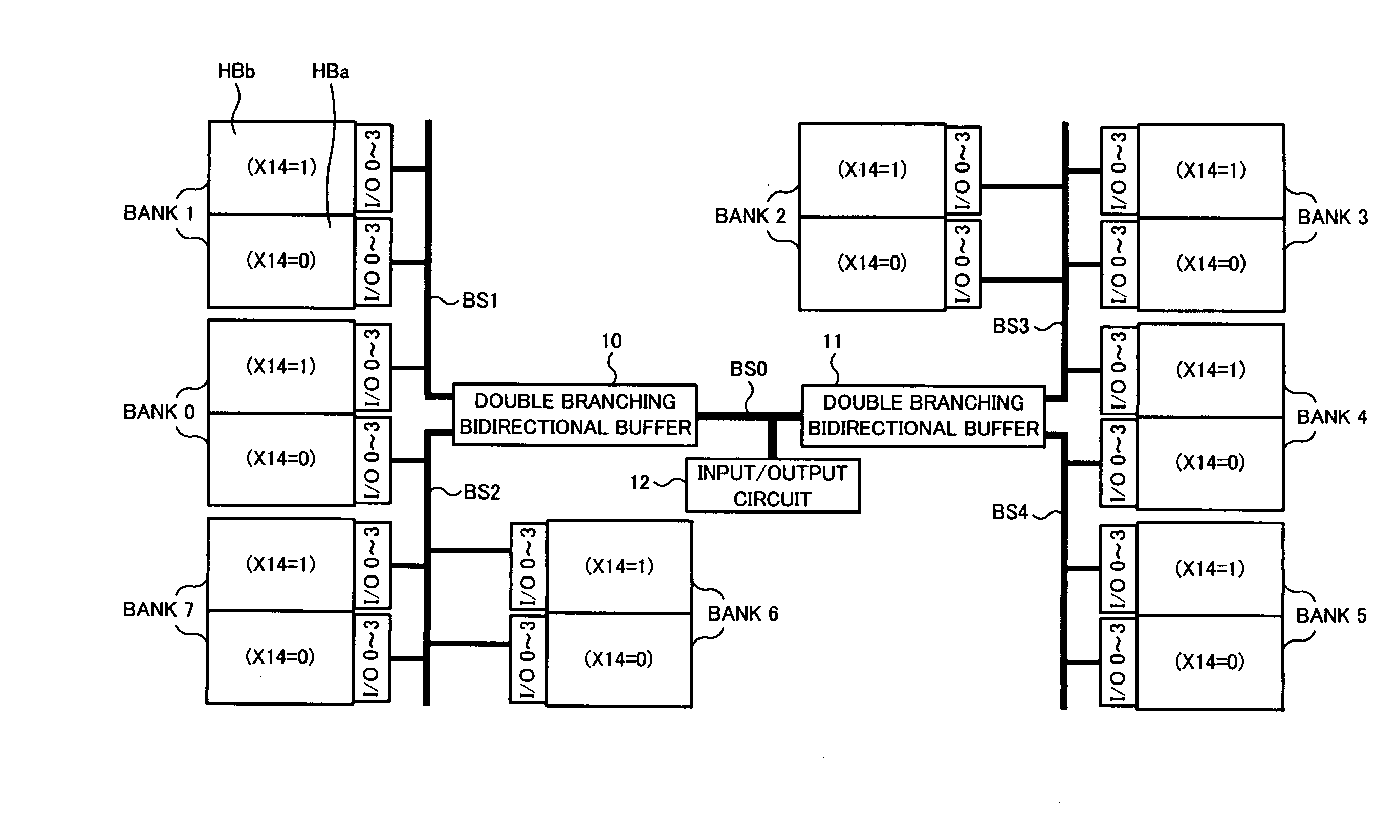
[0040]FIG. 1 is a block diagram showing a principal part of a semiconductor device of a first embodiment. For example, DDR-SDRAM (Double Data Rate-Synchronous DRAM) can be used as the semiconductor memory device of the first embodiment. The semiconductor memory device of the first embodiment includes a memory cell array divided into a plurality of banks, two double branching bidirectional buffers 10 and 11, an input / output circuit 12, a common data bus BS0, and individual data buses BS1, BS2, BS3 and BS4. FIG. 1 shows an example in which the memory cell array is divided into eight banks 0 to 7. Actually, the semiconductor memory device includes many other components, which are omitted in FIG. 1.

[0041]In FIG. 1, each of the eight banks 0 to 7 has the same capacity, and is an independently accessible storage area. Each bank includes many memory cells formed at intersections of a plurality of word lines and a plurality of bit lines. When accessing an arbitrary memory address, a bank se...

second embodiment

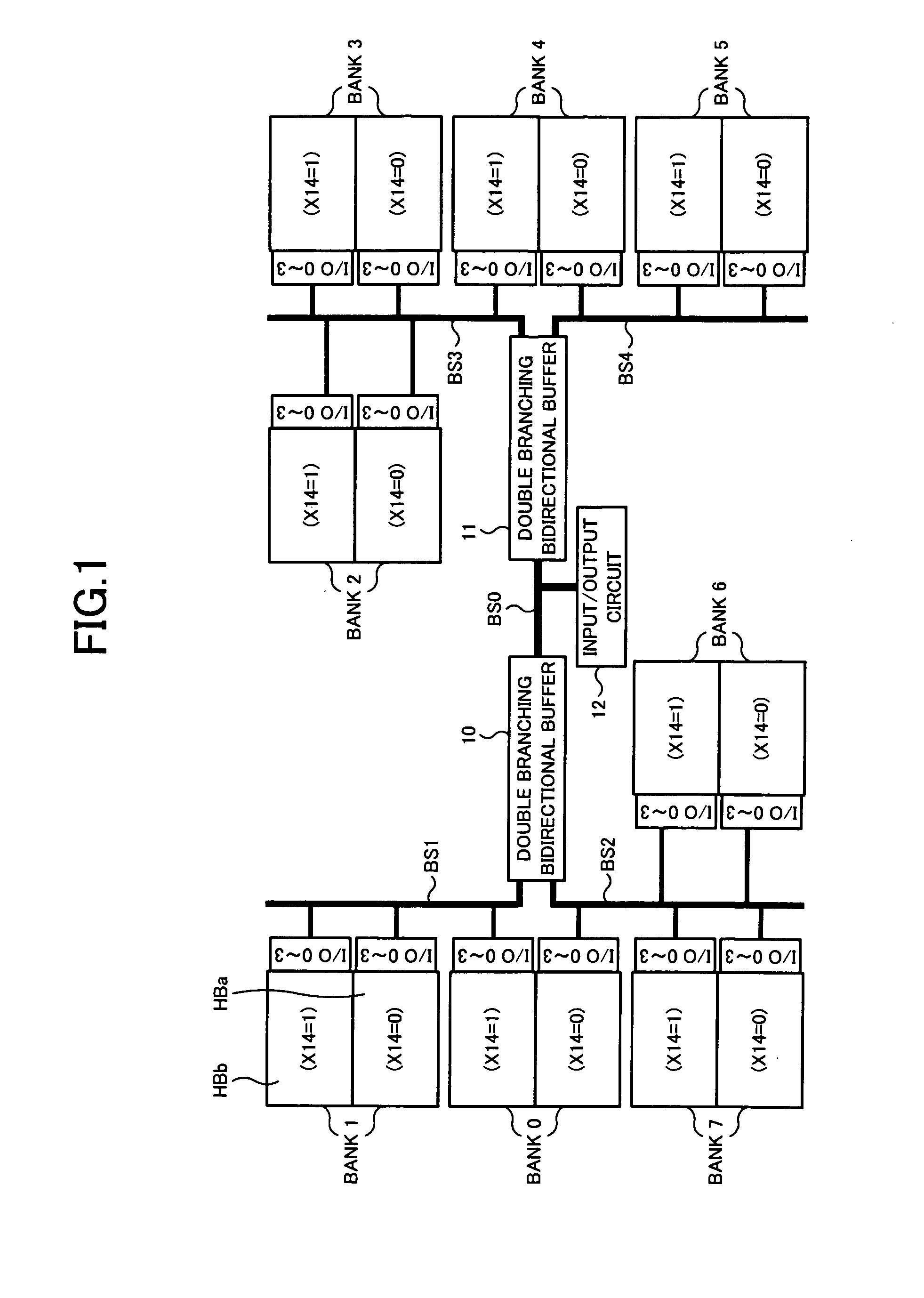
[0074]FIG. 10 is a block diagram showing a principal part of a semiconductor device of a second embodiment. In the second embodiment, since basic components of the semiconductor memory device are common to those in the first embodiment, description of the components having the same numbers as those in FIG. 1 will be omitted. When comparing the second embodiment with the first embodiment, each of eight banks 0 to 7 is partitioned into half bank areas HBx and HBy of upper and lower parts, however a difference exists in that the address information (X14) is not given to the half bank areas HBx and HBy. For example, a case is assumed where the X address is used for other purposes and is not assigned to the address information in each bank. Meanwhile, I / O ports (0 to 3) as four-bit input / output lines are allocated to the lower half bank area HBx, and I / O ports (4 to 7) as the other four-bit input / output lines are allocated to the upper half bank area HBy, respectively, in each bank. Thus...


PUM


Abstract

A semiconductor memory device includes a memory cell array divided into a plurality of areas, a common data bus connected to an input/output circuit, a plurality of individual data buses connected to different areas of the memory cell array through different paths respectively, and a bidirectional buffer connected to the common data bus and the individual data buses. In the semiconductor memory device, the bidirectional buffers data transmitted bidirectionally between the common data bus and a selected one of the individual data buses.

Description

BACKGROUND OF THE INVENTION[0001]1. Field of the Invention[0002]The present invention relates to a semiconductor memory device which transmits data between a memory area for storing data and outside through a data bus, and particularly relates to a semiconductor memory device having a bus configuration in which a bidirectional buffer for buffering data transmitted bidirectionally through the data bus is provided so as to shorten wiring length.[0003]2. Description of Related Art[0004]In recent years, as semiconductor memory devices have been highly integrated, high-speed data transfer rate has been required, and wiring length of a data bus for transmitting data of a memory cell array has been increased. Wiring capacitance and resistance of the data bus increase due to the increase in the wiring length of the data bus, thereby causing delays in data transmission, and it becomes difficult to ensure high-speed data transfer rate.[0005]As measures against the increase in the wiring lengt...

Claims


Application Information

Patent Timeline
Patent Type & Authority Applications(United States)
IPC IPC(8): G11C7/10
CPCG06F13/1673G11C7/1048G11C7/1084G11C7/1057G11C7/1078G11C7/1051
Inventor TAKAHASHI, SUSUMUOISHI, KANJI
Owner LONGITUDE LICENSING LTD
Why Eureka
Try Eureka