Polar modulation transmitter with envelope modulator path switching

a polar modulation transmitter and path switching technology, applied in the field of wireless communication, can solve the problems of reducing efficiency, limiting the battery life of the device, and difficult to improve the power efficiency of conventional rf pas, so as to achieve the effect of reducing the voltage drop across the envelope modulator circuit, reducing the cost of operation, and improving stability and noise isolation

Active Publication Date: 2009-04-30
INTEL CORP
View PDF7 Cites 21 Cited by
  • Summary
  • Abstract
  • Description
  • Claims
  • Application Information

AI Technical Summary

Benefits of technology

[0018]In an exemplary embodiment, the first envelope modulation path includes a p-n-p bipolar junction transistor (BJT), the second envelope modulation path includes an n-p-n BJT, and the predetermined threshold is set so that the first envelope modulation path is selected only at the highest powers required of the RF PA, or when the desired output power is very close to the available supply. When the first envelope modulation path is selected, the p-n-p BJT is employed to provide the envelope modulated supply signal to the power supply input of the RF PA. Use of the p-n-p BJT allows the voltage drop across the envelope modulator circuit to be minimized, which is particularly important at high output power levels. For times when the power is below the predetermined threshold, the second envelope modulation path is selected. When the second envelope modulation path is selected, the n-p-n BJT is employed to provide the envelope modulated supply signal to the power supply input of the RF PA. Use of the n-p-n BJT at these relatively lower power levels affords improved stability and noise isolation. Hence, switching between the first and second envelope modulation paths, depending on the power requirements of the RF PA, provides greater stability and dynamic range, while still offering efficient power transfer at higher power levels.
[0019]According to one aspect of the invention, the envelope modulator circuit may be adapted to include a DC-to-DC converter that lowers the supply voltage provided to the second envelope modulation path when the second envelope modulation path is selected (i.e., when the n-p-n BJT is ON and the p-n-p BJT is OFF). Lowering the supply voltage substantially reduces the power dissipated by the n-p-n BJT as the n-p-n BJT transfers the envelope modulated supply signal to the power supply input of the RF PA.

Problems solved by technology

These additional features can severely limit the device's battery life.
Unfortunately, because conventional power amplifier circuits must operate linearly, but are not very efficient when configured to do so, improving the power efficiency of conventional RF PAs has been a very difficult problem.
The immediate consequence of this linearization effort is a reduction in efficiency.
These drawbacks relate in particular to use of the p-n-p type BJT 304, which when operating at low powers can be susceptible to noise.
This susceptibility to noise is highly undesirable, since noise can cause distortions in the RF output signal of the RF PA 114.
However, the gain of practical op-amps is frequency dependent, and decreases and approaches unity as the frequency of its input signal (in this case, the AM signal) increases.
When the phase shift reaches 180° the amplifier can become unstable and can even begin to oscillate.
Oscillations render the amplifier circuit unsuitable for its intended purpose, since, during oscillations, the output of the amplifier bears no relationship to the AM signal applied to the amplifier's input.
Therefore, in addition to the problem of being susceptible to noise at low output power levels, the envelope modulator circuit 108 in FIG. 3 is beset with stability concerns which limit the modulator's dynamic range.

Method used


Image

  • Polar modulation transmitter with envelope modulator path switching
  • Polar modulation transmitter with envelope modulator path switching
  • Polar modulation transmitter with envelope modulator path switching

Examples


Embodiment Construction

[0028]Those of ordinary skill in the art will realize that the following detailed description of the present invention is illustrative only and is not intended to be in any way limiting. Other embodiments of the present invention will readily suggest themselves to such skilled persons having the benefit of this disclosure. Reference will now be made in detail to implementations of the present invention as illustrated in the accompanying drawings. The same reference indicators will be used throughout the drawings and the following detailed description to refer to the same or like parts.

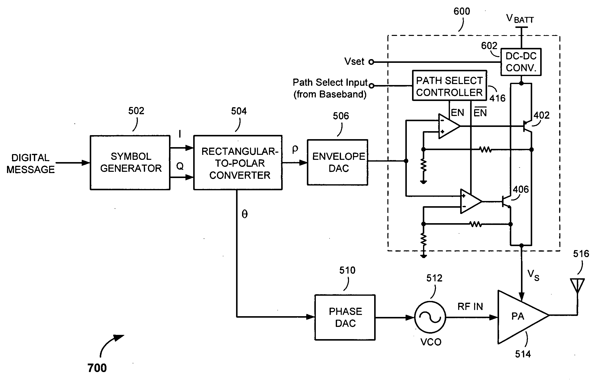
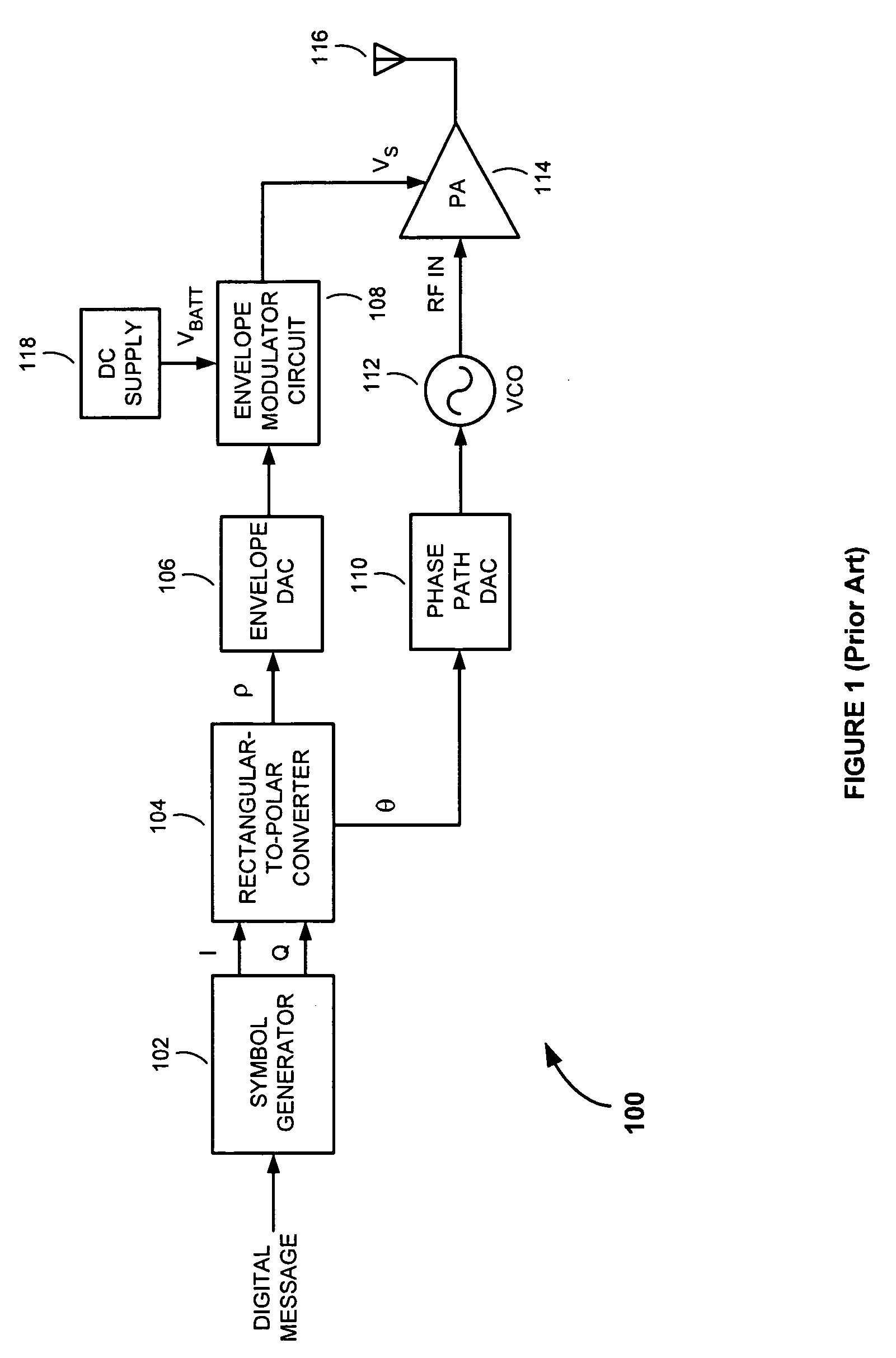
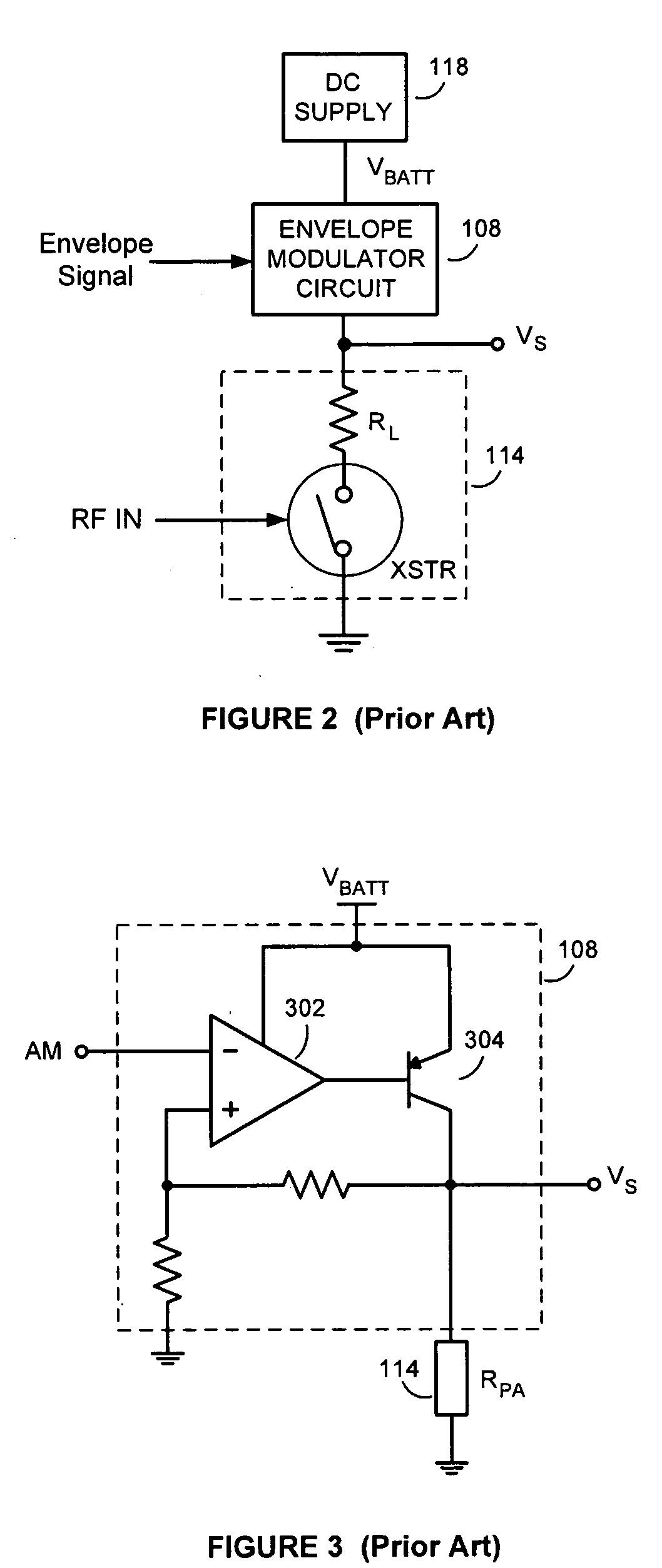
[0029]Referring first to FIG. 4, there is shown an envelope modulator circuit 400 for use in the amplitude path of a polar modulation transmitter, in accordance with an embodiment of the present invention. The envelope modulator circuit 400 comprises first and second parallel power supply paths selectively configured to supply power to the power supply port of an RF PA (represented as a load 401 having...


PUM


Abstract

Methods and apparatus for controlling power in a polar modulation transmitter. An exemplary polar modulation transmitter includes a radio frequency power amplifier (RF PA), a phase path having circuitry operable to generate a constant amplitude phase modulated signal, and an amplitude path including an envelope modulator circuit having first and second envelope modulation paths. The RF phase modulated signal is applied to an RF input of the RF PA, while an envelope modulated power supply signal generated by a selected one of the first and second envelope modulation paths is coupled to a power supply input of the RF PA. The second envelope modulation path is selected during times when the power required by the RF PA is below some predetermined power level. During times when the RF PA requires power above the predetermined power level, the first envelope modulation path is selected.

Description

CROSS-REFERENCE TO RELATED APPLICATIONS[0001]This patent application claims the benefit of U.S. Provisional Patent Application No. 60 / 983,154, filed on Oct. 26, 2007, the disclosure of which is hereby incorporated by reference.FIELD OF THE INVENTION[0002]The present invention relates to wireless communications. More specifically, the present invention relates to power control in polar modulation transmitters.BACKGROUND OF THE INVENTION[0003]Portable wireless communication devices, such as cellular handsets, personal digital assistants (PDAs) and hand-held computers, are becoming smaller and lighter with each new generation of wireless communication technology. They are also becoming more technically sophisticated, and currently often provide or support, in addition to traditional voice communications, features such as built-in cameras, Bluetooth connectivity, text and instant messaging, and mini browsers for surfing the Internet. These additional features can severely limit the devi...

Claims


Application Information

Patent Timeline
Patent Type & Authority Applications(United States)
IPC IPC(8): H04B1/04H04B1/02
CPCH03F1/0227H03F1/0244H04B1/0483H03F2200/451H03F2200/504H03F3/24
Inventor DUNSMORE, MARNIEMCCUNE, JR., EARL W.DO, GARY
Owner INTEL CORP
Why Eureka
Try Eureka