Implementation of One Time Programmable Memory with Embedded Flash Memory in a System-on-Chip

a one-time programmable memory and embedded flash memory technology, applied in the field of system-on-chip security, can solve the problems of inability to use security functions, increase costs, and increase costs of adding otp

Active Publication Date: 2009-04-30
MICROCHIP TECH INC
View PDF12 Cites 41 Cited by
  • Summary
  • Abstract
  • Description
  • Claims
  • Application Information

AI Technical Summary

Benefits of technology

[0012]In some embodiments, the SoC also includes a controller and a flash memory controller coupled to the flash memory array for reading from and writing to the flash memory array. Latching at least a portion of the OTP block may include: in response to deasserting system reset, holding the controller in reset, sending an address of the OTP block to the flash memory array as input, sequencing the flash memory array to read data from the OTP block at the address, and latching the data read from the OTP block in the volatile memory, including asserting the OTP write inhibit bit. Thus, in some embodiments, the controller may be prevented from doing anything (e.g., reading or writing to flash memory) while the OTP memory block is being initialized and the data are latched. In some embodiments, the flash memory controller may perform this latching of the data.

Problems solved by technology

Moreover, many of these systems include security features that utilize one time programmable (OTP) memory that cannot be reprogrammed or erased.
If an SoC requires a large flash memory, adding OTP can increase costs, since OTP typically requires different processing in manufacture than flash memory, as well as additional area.
However, as currently used, flash memory can be erased, which means it cannot be used for security functions, since an attack could erase the flash memory, thereby eliminating the security function.

Method used


Image

  • Implementation of One Time Programmable Memory with Embedded Flash Memory in a System-on-Chip
  • Implementation of One Time Programmable Memory with Embedded Flash Memory in a System-on-Chip
  • Implementation of One Time Programmable Memory with Embedded Flash Memory in a System-on-Chip

Examples


Embodiment Construction

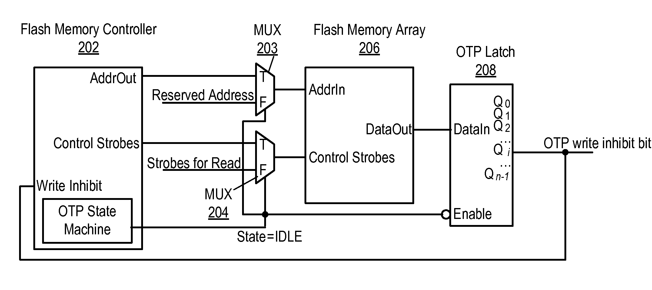
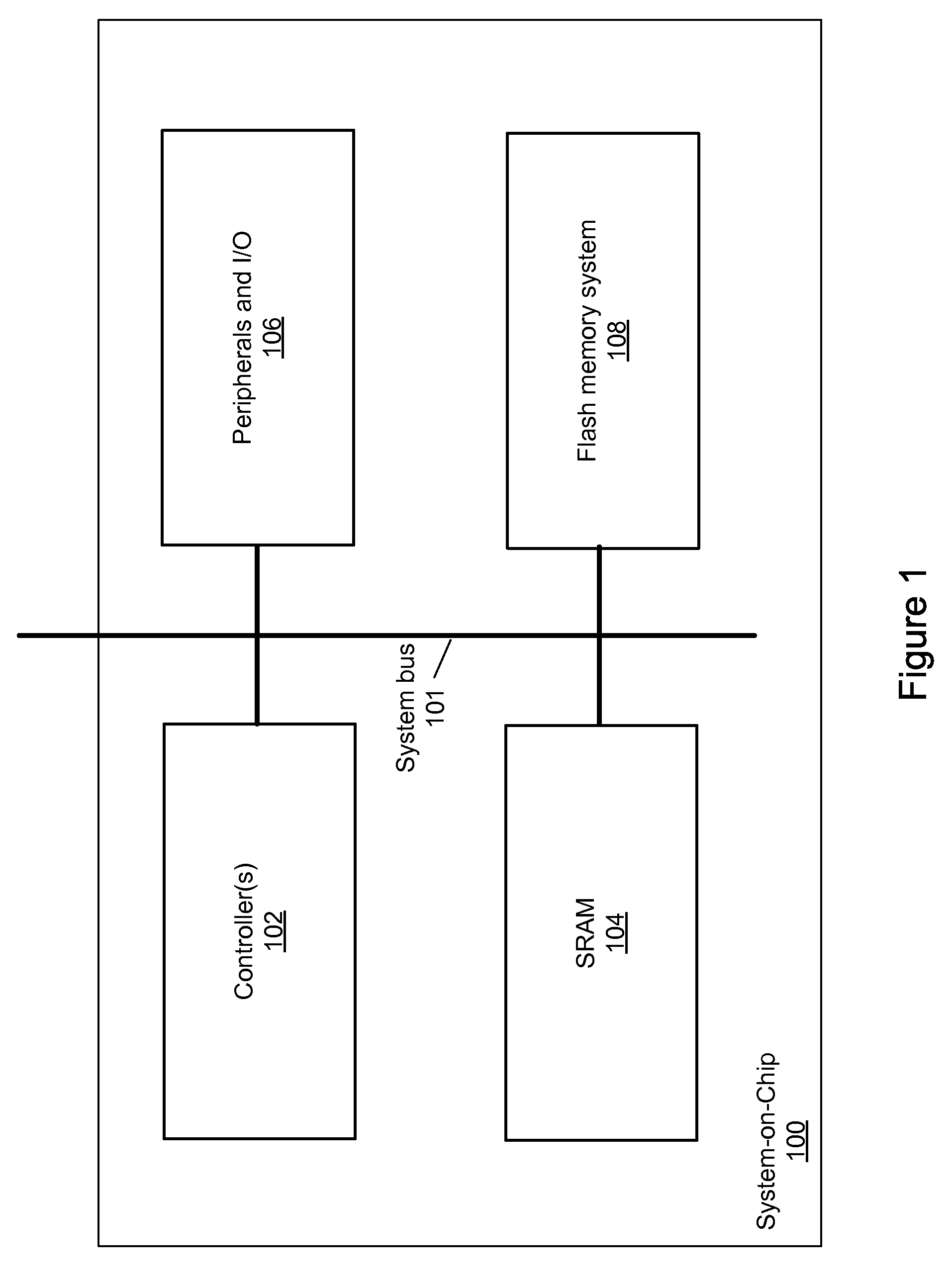
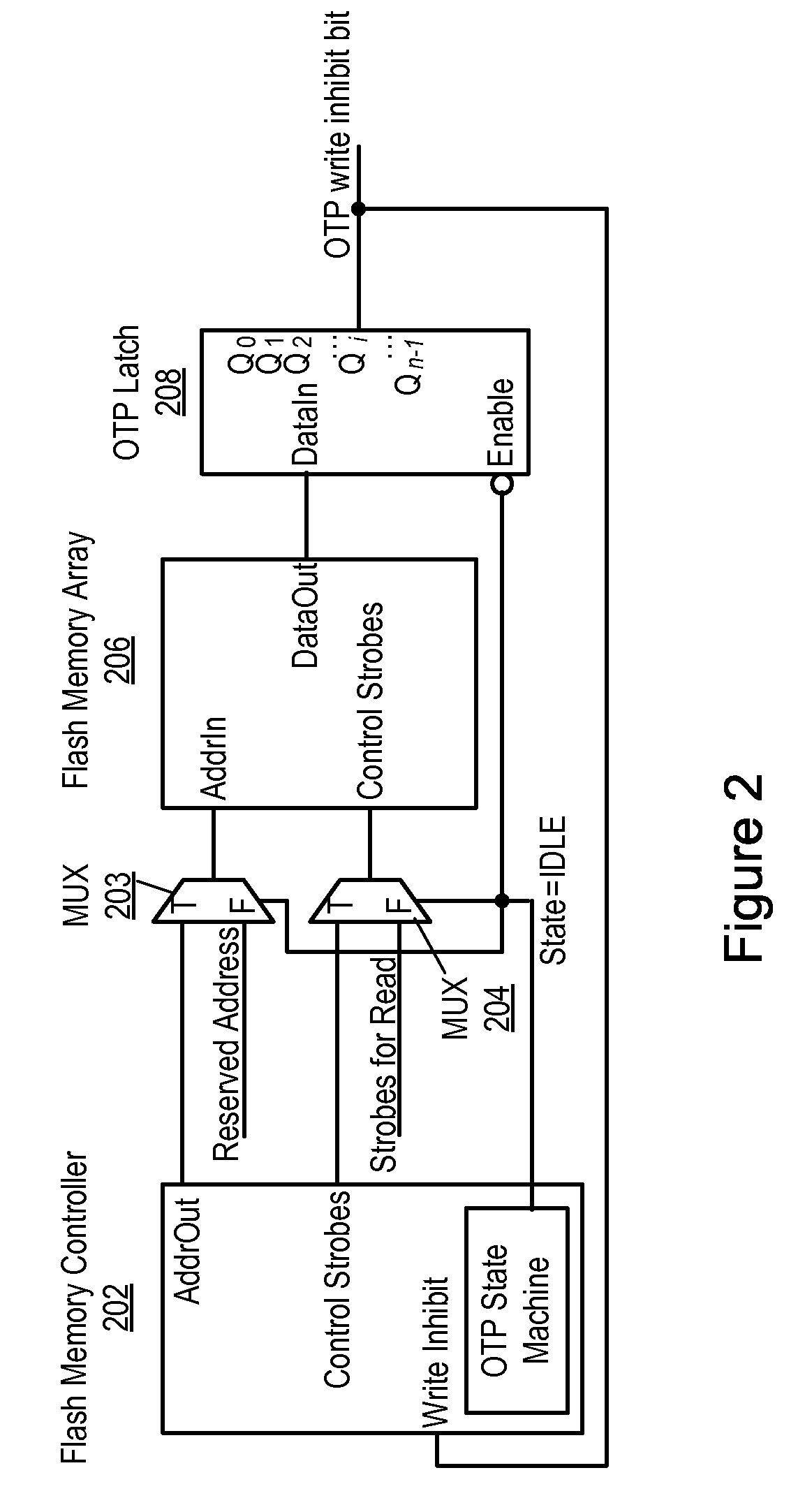
[0030]Below are described various embodiments of a system and method for implementing one time programmable (OTP) memory with embedded flash memory, referred to herein as “flash OTP”, in a System-on-Chip (SoC). The flash OTP may be useful in any SoC that uses OTP memory, e.g., for security functions, power-up / reset, and so forth.

[0031]As used herein, a “set of instructions” may refer to one or more instructions. More specifically, in some embodiments, “instructions” may refer to programming code, software, and / or functions implemented in the form of a code that is executable by a controller, microprocessor, and / or custom logic circuit adapted to execute these instructions. In some embodiments, these instructions may comprise device drivers, control software, and / or machine code.

[0032]As used herein, a “controller” refers to any type of processor or controller, such as a central processing unit (CPU), microprocessor, embedded controller, DMA (direct memory access) controller, or comb...


PUM


Abstract

System and method for implementing one time programmable (OTP) memory using embedded flash memory. A system-on-chip (SoC) includes a cleared flash memory array that includes an OTP block, including an OTP write inhibit field that is initially deasserted, a flash memory controller, and a controller. Data are written to the OTP block, including setting the OTP write inhibit field to signify prohibition of subsequent writes to the OTP block. The SoC is power cycled, and, in response, at least a portion of the OTP block is latched in a volatile memory, including asserting an OTP write inhibit bit based on the OTP write inhibit field, after which the OTP block is not writeable. In response to each subsequent power cycling, the controller is held in reset, the latching is performed, the controller is released from reset, and the flash array, now write protected, is configured to be controlled by the controller.

Description

BACKGROUND OF THE INVENTION[0001]1. Field of the Invention[0002]This invention relates generally to the field of System-on-Chip (SoC) security, and more specifically to implementation of one time programmable memory using embedded flash memory on an SoC.[0003]2. Description of the Related Art[0004]Increasingly, sophisticated hardware systems are implemented on single computer chips. Such a system is referred to as a System-on-Chip (SoC). An SoC generally includes at least one controller and memory, and is generally required to perform auxiliary functions for the system, such as initialization and reset functionality. Moreover, many of these systems include security features that utilize one time programmable (OTP) memory that cannot be reprogrammed or erased. Because OTP memory cannot be modified (after its initial programming), it is suitable for such security functions.[0005]Flash memory, in contrast, can be erased. If an SoC requires a large flash memory, adding OTP can increase ...

Claims


Application Information

Patent Timeline
Patent Type & Authority Applications(United States)
IPC IPC(8): G06F12/02
CPCG06F2212/2022G06F12/1433
Inventor BERENBAUM, ALAN D.WAHLER, RICHARD E.WEISS, RAPHAEL
Owner MICROCHIP TECH INC
Why Eureka
Try Eureka