Solving Via-Misalignment Issues in Interconnect Structures Having Air-Gaps

Active Publication Date: 2009-05-07
TAIWAN SEMICON MFG CO LTD
View PDF5 Cites 57 Cited by
  • Summary
  • Abstract
  • Description
  • Claims
  • Application Information

AI Technical Summary

Benefits of technology

[0013]The advantageous features of the present invention include reduced parasitic capacitance, reduc

Problems solved by technology

In the past, such reductions were limited only by the ability to define the structures photo-lithographically, and device geometries having smaller dimensions create new limiting factors.
This increased capacitance results in increased power consumption and increased resistive-capacitive (RC) delay.
Furthermore, air-gaps are formed to further reduce effective k values.
Although the formation of

Method used


Image

  • Solving Via-Misalignment Issues in Interconnect Structures Having Air-Gaps
  • Solving Via-Misalignment Issues in Interconnect Structures Having Air-Gaps
  • Solving Via-Misalignment Issues in Interconnect Structures Having Air-Gaps

Examples


Example

[0018]The making and using of the presently preferred embodiments are discussed in detail below. It should be appreciated, however, that the present invention provides many applicable inventive concepts that can be embodied in a wide variety of specific contexts. The specific embodiments discussed are merely illustrative of specific ways to make and use the invention, and do not limit the scope of the invention.

[0019]The present invention provides methods for reducing parasitic capacitances in interconnect structures and for reducing the adverse effects of via-misalignment in the formation of interconnect structures. The intermediate stages of manufacturing preferred embodiments of the present invention are illustrated. Throughout the various views and illustrative embodiments of the present invention, like reference numbers are used to designate like elements.

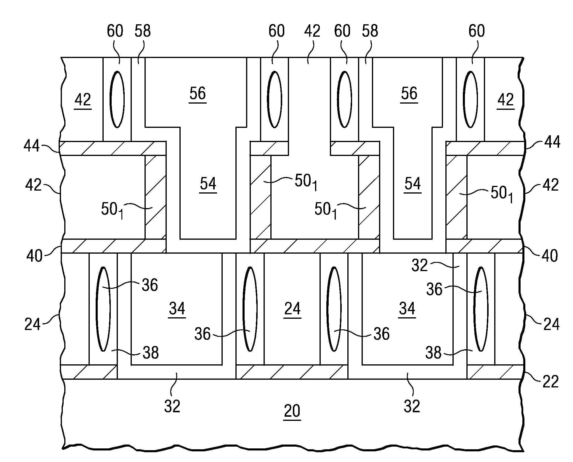
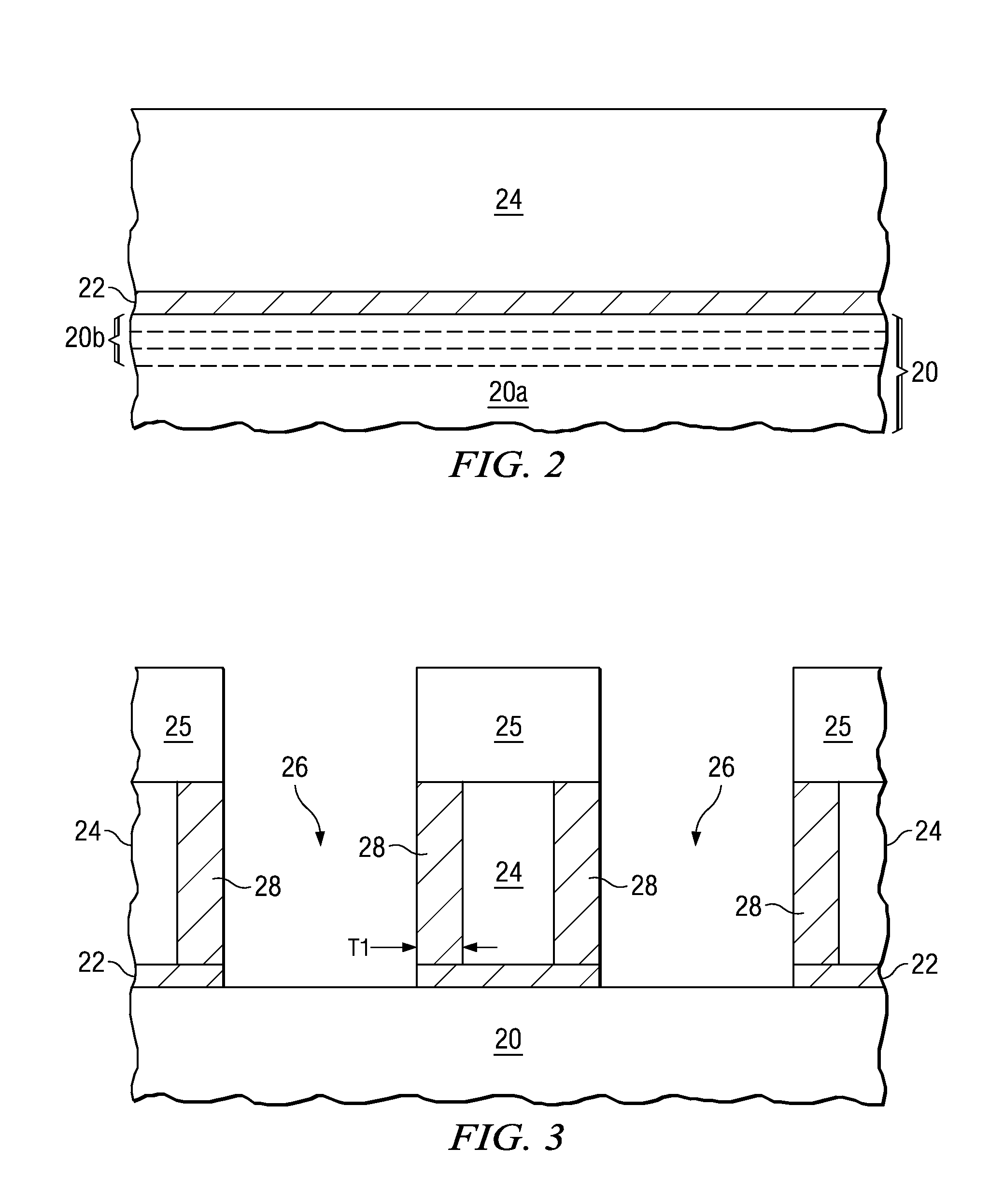
[0020]FIGS. 2 through 10B are cross-sectional views of intermediate stages for forming a single damascene structure.FIG. 2 i...


PUM


Abstract

An integrated circuit structure is provided. The integrated circuit structure includes a semiconductor substrate; and a metallization layer over the semiconductor substrate. The metallization layer includes a conductive line; a low-k dielectric region adjacent and horizontally spaced apart from the conductive line by a space; and a filler dielectric material filling at least a portion of the space, wherein the filler dielectric material and the low-k dielectric region are formed of different materials. The integrated circuit structure further includes a capping layer over and adjoining the filler dielectric material and the low-k dielectric region. The filler dielectric material has a dielectric constant (k value) less than a k value of the capping layer.

Description

TECHNICAL FIELD[0001]This invention relates generally to integrated circuits, and more particularly to methods for reducing the effects of damaged low-k dielectric layers.BACKGROUND[0002]As the semiconductor industry introduces new generations of integrated circuits (IC) having higher performance and more functionality, the density of the elements forming the ICs increases, while the dimensions, sizes, and spacing between components or elements are reduced. In the past, such reductions were limited only by the ability to define the structures photo-lithographically, and device geometries having smaller dimensions create new limiting factors. For example, for any two adjacent conductive features, as the distance between the conductive features decreases, the resulting capacitance (a function of the dielectric constant (k value) of the insulating material divided by the distance between the conductive features) increases. This increased capacitance results in increased power consumpti...

Claims


Application Information

Patent Timeline
IPC IPC(8): H01L23/52
CPCH01L21/76807H01L21/7682H01L21/76831H01L21/76835H01L2924/0002H01L23/5222H01L2924/00
Inventor CHEN, HSIEN-WEI
Owner TAIWAN SEMICON MFG CO LTD
Why Eureka
Try Eureka