

Semiconductor memory device using bus inversion scheme
a technology of semiconductor memory and bus inversion scheme, which is applied in the direction of information storage, static storage, digital storage, etc., can solve the problems of increasing power consumption, unsatisfactory input/output speed of address or command signal, and a large amount of current consumption, so as to prevent a degradation of setup/hold time, increase operation speed, and reduce power consumption
- Summary
- Abstract
- Description
- Claims
- Application Information
AI Technical Summary
Benefits of technology
Problems solved by technology
Method used
Image

Examples
Embodiment Construction
[0021]Hereinafter, a semiconductor memory device using a bus inversion scheme in accordance with the present invention will be described in detail with reference to the accompanying drawings.
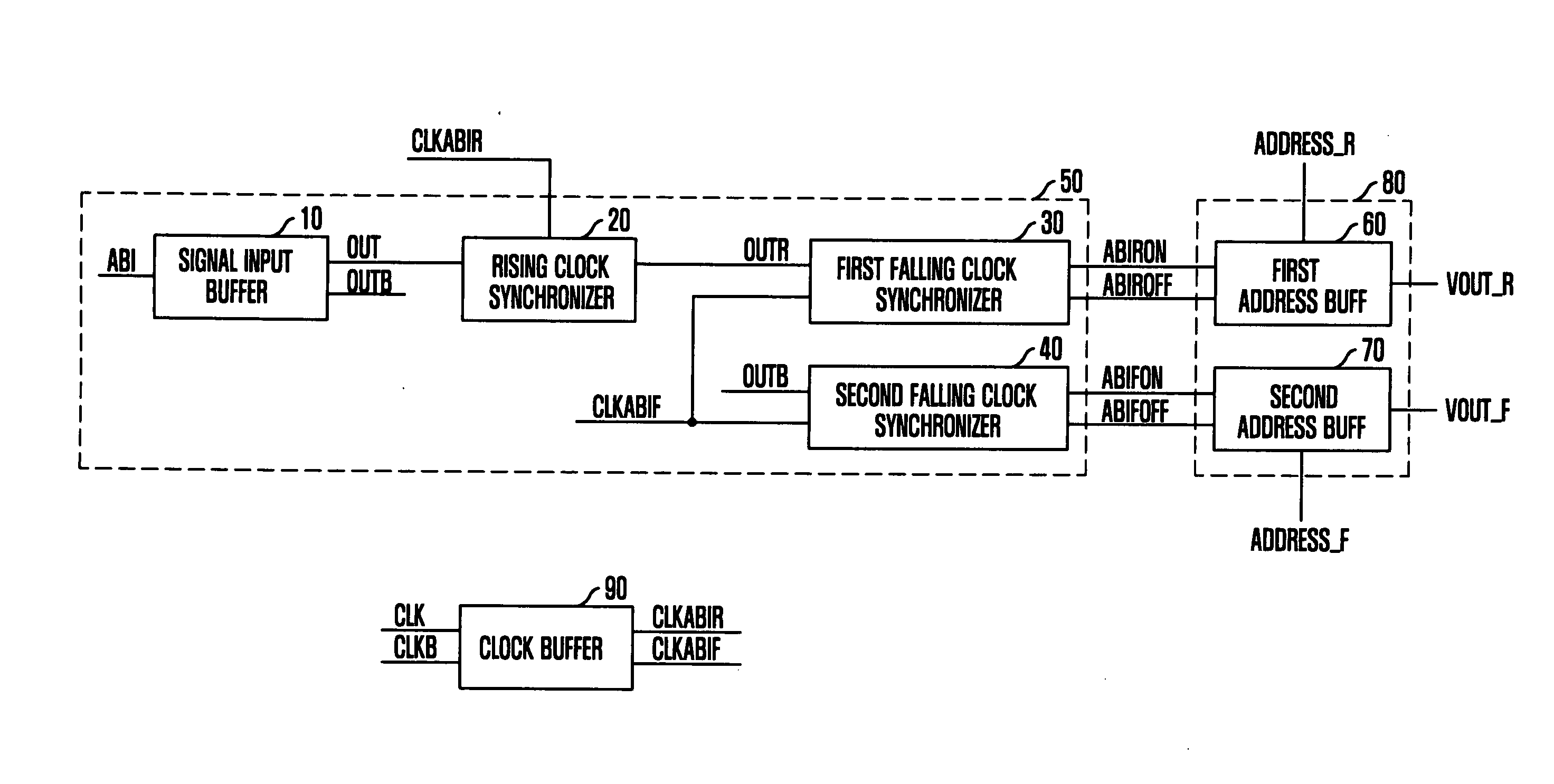
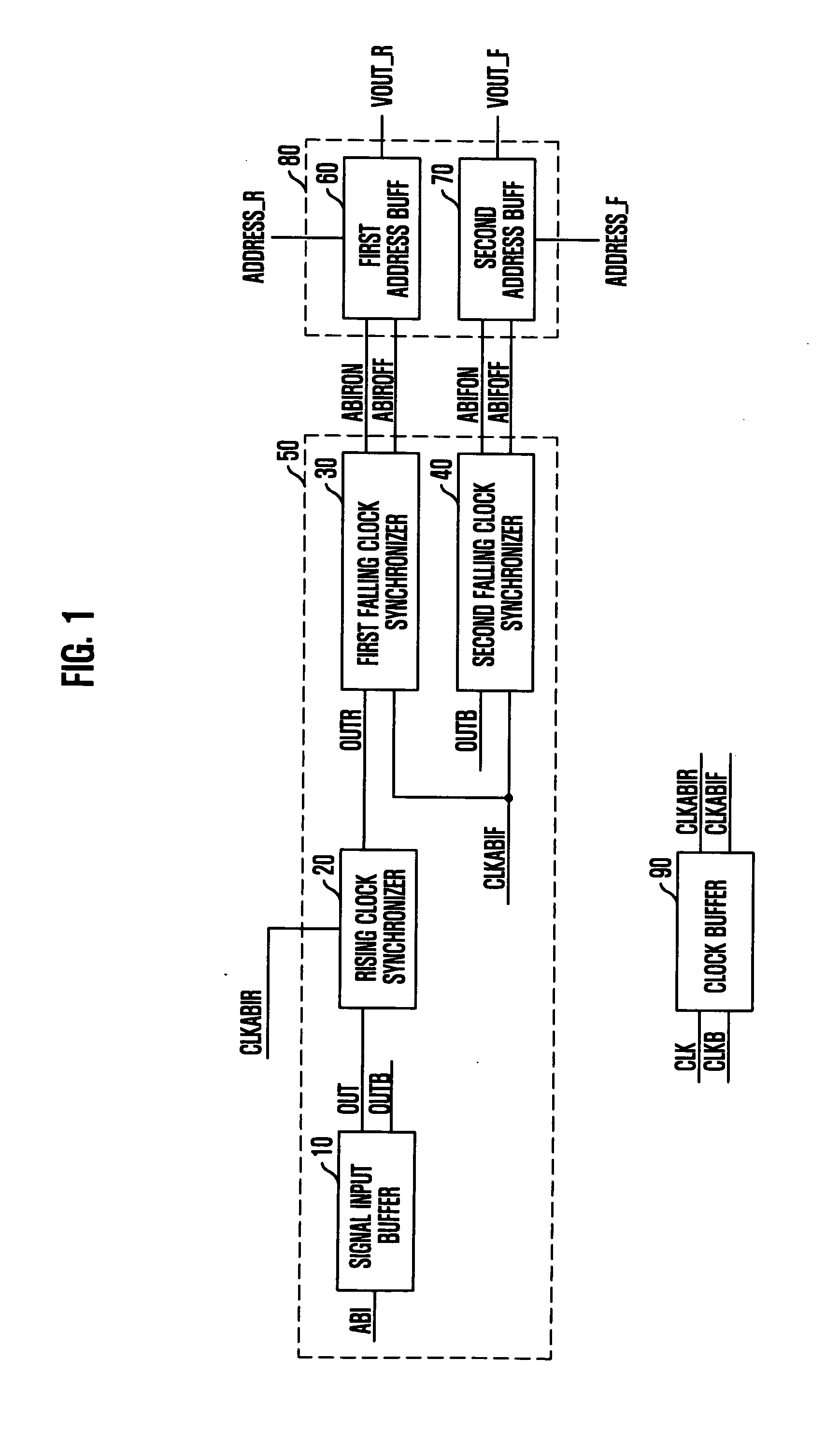
[0022]FIG. 1 is a block diagram of a semiconductor memory device in accordance with an embodiment of the present invention.
[0023]Referring to FIG. 1, the semiconductor memory device includes a bus inversion decoding block 50 and an address buffer block 80. The bus inversion decoding block 50 includes a signal input buffer 10, a rising clock synchronizer 20, and first and second falling clock synchronizers 30 and 40. The bus inversion decoding block 50 decodes an indication control signal ABI and controls the address bus block 80. The address buffer block 80 includes first and second address buffers 60 and 70. The address buffer block 80 transfers addresses according to a control signal outputted from the bus inversion decoding unit 50.
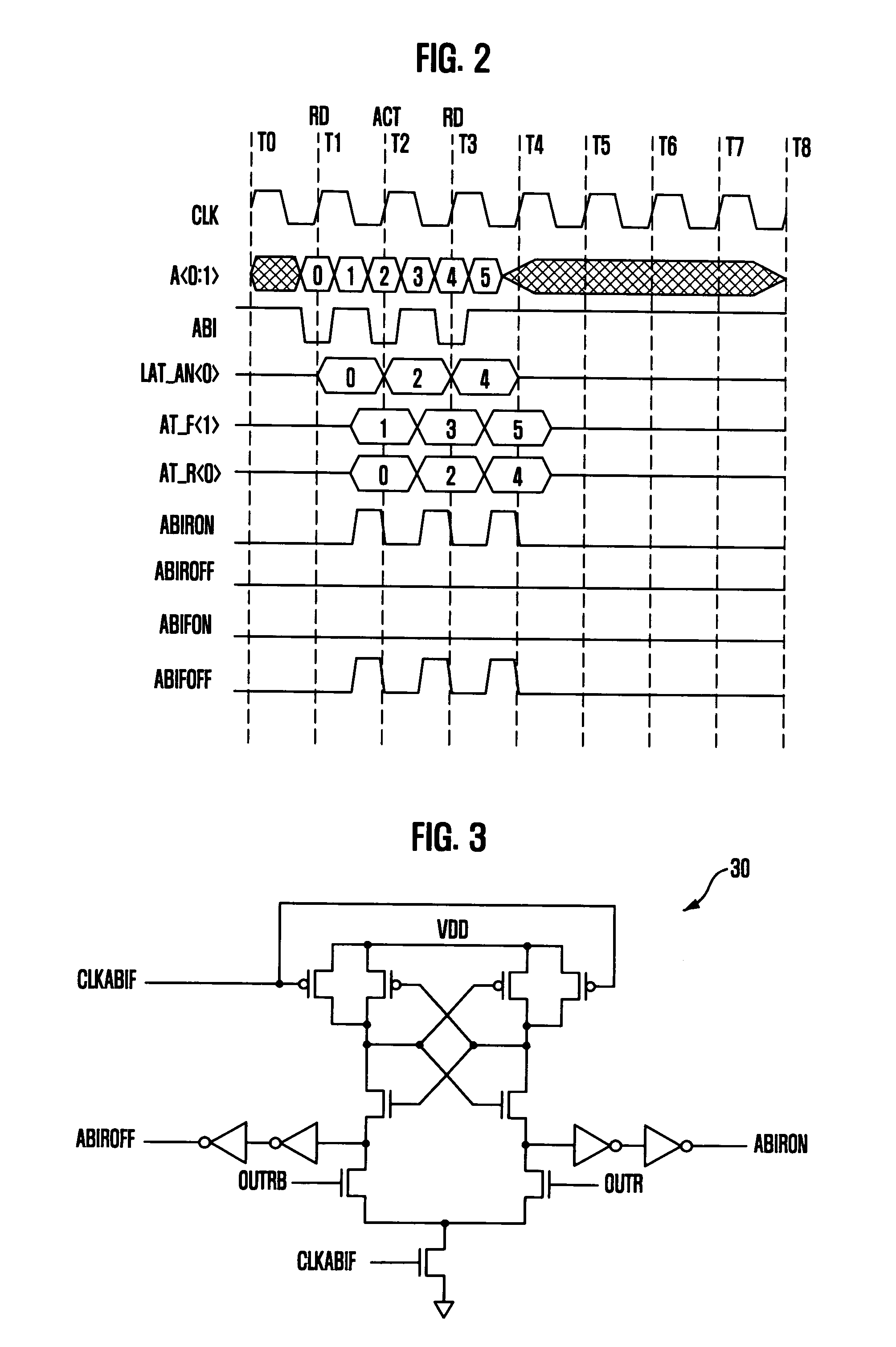
[0024]The signal input buffer 10 receives the indication cont...
PUM
 Abstract
Description
Claims
Application Information