Semiconductor device manufacturing method and substrate processing apparatus

a technology of semiconductor devices and processing equipment, which is applied in the direction of lighting and heating equipment, crystal growth process, polycrystalline material growth, etc., can solve the problems that components might possibly contaminate the wafer surface with impurities, and achieve the effect of satisfying cleaning effect, increasing thermal budget and heat damage to the substrate, and high quality

Active Publication Date: 2009-05-07
KOKUSA ELECTRIC CO LTD
View PDF4 Cites 20 Cited by
  • Summary
  • Abstract
  • Description
  • Claims
  • Application Information

AI Technical Summary

Benefits of technology

[0076]The first aspect (1) of the invention renders the effect that a satisfactory cleaning effect can be obtained at a low temperature so that an increased thermal budget and heat damage to the substrates can be prevented to form a high quality interface with a low-oxygen and low-carbon density between a substrate and a thin film.

Problems solved by technology

These components might possibly contaminate the wafer surface with impurities such as organic substances while drawing a vacuum.

Method used


Image

  • Semiconductor device manufacturing method and substrate processing apparatus
  • Semiconductor device manufacturing method and substrate processing apparatus
  • Semiconductor device manufacturing method and substrate processing apparatus

Examples


first embodiment

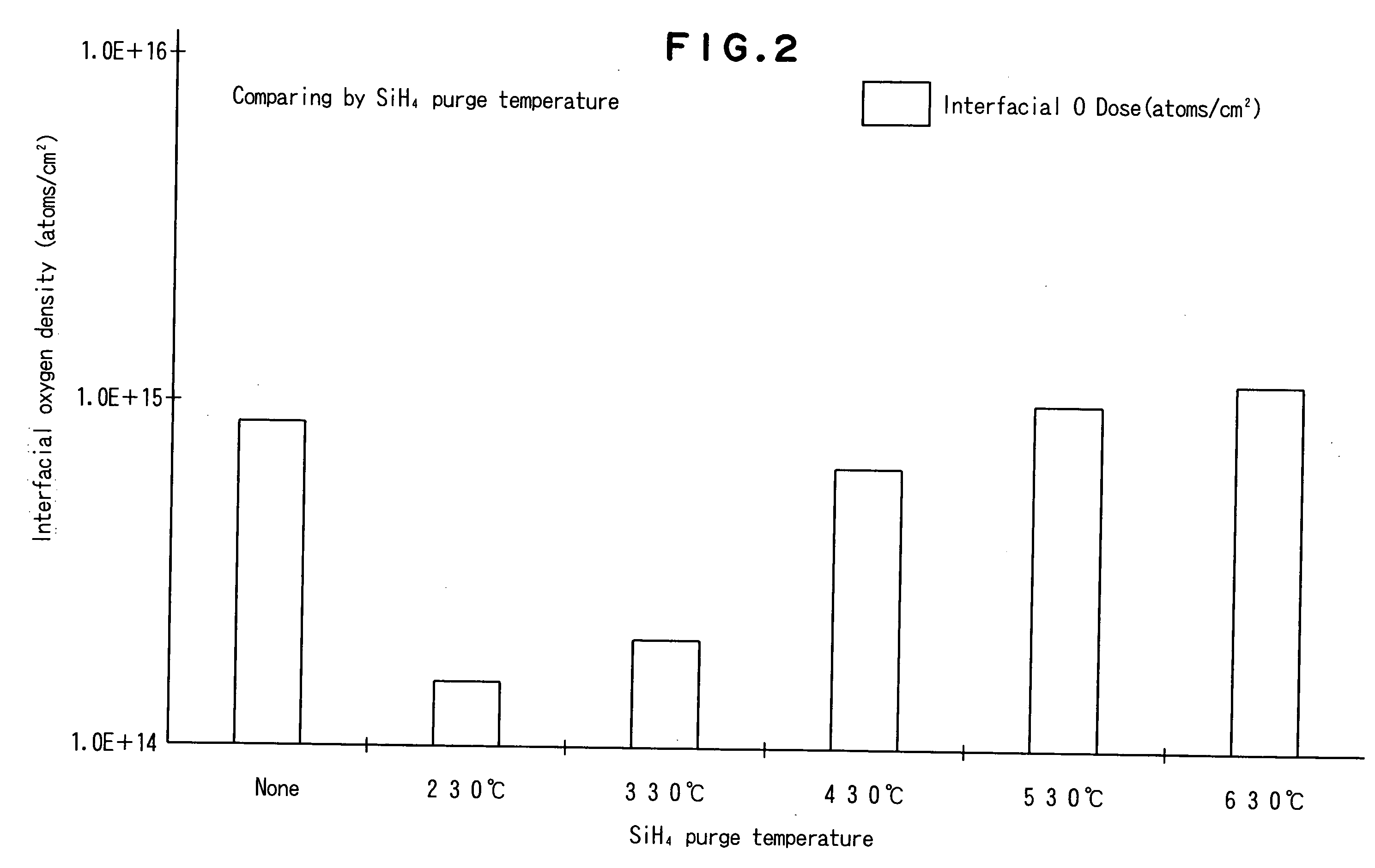
[0150]Experiments performed for determining pressure dependence and temperature dependence of the interfacial oxygen density (concentration) in SiH4 purge are described next for the first embodiment.

[0151]The electrodes extending from the DRAM source and drain are used as one example of a semiconductor device requiring a low oxygen density interface. This interfacial characteristic is referred to as contact resistance. The tinier the natural oxidized film in this section, the less the contact resistance and the better the electrical characteristics.

[0152]In the experiment to evaluate this embodiment, the interfacial characteristics between the D-polysilicon film (phosphorus dope silicon film) and D-polysilicon film (phosphorus dope silicon film), were measured with SIMS (Secondary Ionization Mass Spectrometer).

[0153]The evaluation device was the apparatus of the above embodiment. In other words, a load-lock type apparatus effective in reduction of the interfacial oxygen density was ...

second embodiment

[0177]Experiments for determining the temperature dependence of the contact resistance in SiH4 purge are described next for the second embodiment.

[0178]The second embodiment evaluates the interfacial contact resistance by utilizing actual devices based on SIMS evaluation results of the first embodiment.

[0179]The SIMS results of the first embodiment showed that an SiH4 purge proved effective at a low temperature and high vacuum so that the pressure here was fixed at 10 Pa using a TMP, and the temperature was set to the two cases of 330° C. and 430° C. which are lower than the film-forming temperature (530° C.).

[0180]FIG. 4 shows the temperature dependence of the interfacial contact resistance in the SiH4 purge.

[0181]The horizontal axis indicates the SiH4 purge temperature (° C.), and the vertical axis indicates the interfacial contact resistance (ohms / pieces).

[0182]In this evaluation, the SiH4 purge temperature was changed to 330° C. and 430° C. as described previously.

[0183]The “Non...

third embodiment

[0185]Next in the third embodiment, an experiment performed to find the time dependence of the interfacial oxygen density in the SiH4 purge in the time from setting the wafer in the furnace to starting of the SiH4 purge event is described.

[0186]The time dependence (SIMS result) of the interfacial oxygen density in the time from the end of placing the wafer in the furnace to the SiH4 purge event is shown in FIG. 5.

[0187]The horizontal axis indicates the time (minutes) from completing the placement of the wafers in the furnace to the SiH4 purge event. The vertical axis indicates the interfacial oxygen density (atoms / cm2).

[0188]As shown in FIG. 5, in this evaluation the time from placing wafers in the furnace up to the SiH4 purge event was changed to 50 minutes and 15 minutes.

[0189]One can see in FIG. 5, that the shorter of the times from placing wafers in the furnace up to the SiH4 purge event possesses a slight interfacial oxygen density. That result is due to the following reasons.

[...


PUM

PropertyMeasurementUnit
pressureaaaaaaaaaa
pressureaaaaaaaaaa
temperatureaaaaaaaaaa

Abstract

A high quality interface is formed at a low oxygen-carbon density between a substrate and a thin film while preventing heat damage on the substrate and increase of thermal budget. This method includes a step of loading a wafer into a reaction furnace, a step of pretreating the wafer in the reaction furnace, a step of performing a main processing of the pretreated wafer in the reaction furnace, and a step of unloading the wafer from the reaction furnace after the main processing. Hydrogen gas is continuously supplied to the reaction furnace in the period from the end of the pretreating step to the start of the main processing and at least during vacuum-exhausting an interior of the reaction furnace.

Description

TECHNICAL FIELD[0001]The present invention relates to a semiconductor device manufacturing method and substrate processing apparatus, and is effective for example in use for processes for forming thin films on semiconductor wafers (hereafter called wafers) for forming a semiconductor integrated circuit device containing semiconductor devices in methods for manufacturing a semiconductor integrated circuit device (hereafter called IC), and relates in particular to technology for forming a high quality interface between the silicon wafer and the thin film.BACKGROUND ART[0002]In IC manufacturing methods, thin films are formed on wafers by the depressurizing CVD (chemical vapor deposition) method.[0003]In recent years, in order to resolve problems when loading the wafer into the reaction furnace such as semiconductor deterioration due to impurities adhering to the semiconductor or an increase in the natural oxidation film, a method is utilized where a prechamber is installed at a stage p...

Claims


Application Information

Patent Timeline
Patent Type & Authority Applications(United States)
IPC IPC(8): H01L21/02F23N5/22
CPCC23C16/4408C23C16/54C30B25/02C30B29/06H01L21/67109H01L21/02532H01L21/0262H01L21/02658H01L21/67017H01L21/02046H01L21/205
Inventor OZAKI, TAKASHIKASAHARA, OSAMUNODA, TAKAAKIMAEDA, KIYOHIKOMORIYA, ATSUSHISAKAMOTO, MINORU
Owner KOKUSA ELECTRIC CO LTD
Why Eureka
Try Eureka