Pulse train annealing method and apparatus

a technology of annealing method and annealing apparatus, which is applied in the direction of manufacturing tools, lighting and heating apparatus, furniture, etc., can solve the problems of increasing switching speed, unsatisfactory processing, and increasing problems

Inactive Publication Date: 2009-05-14
APPLIED MATERIALS INC
View PDF37 Cites 78 Cited by
  • Summary
  • Abstract
  • Description
  • Claims
  • Application Information

AI Technical Summary

Problems solved by technology

Although widely used, such processes are not ideal because they ramp the temperature of the wafer too slowly and expose the wafer to elevated temperatures for too long.
These problems become more severe with increasing wafer sizes, increasing switching speeds, and / or decreasing feature sizes.
Such broad diffusion reduces the electrical performance of the doped regions by reducing concentration of dopants and spreading them through a larger region of the substrate.
This limits how fast one can heat and cool the substrate.
Moreover, once the entire substrate is at an elevated temperature, heat can only dissipate into the surrounding space or structures.
As a result, today's state of the art RTP systems struggle to achieve a 400° C. / s ramp-up rate and a 150° C. / s ramp-down rate.
In order to deliver enough energy to result in substantial annealing, however, large energy densities are required.
Delivering enough energy to substantially anneal the substrate in a single short-duration pulse often results in significant damage to its surface.
Moreover, delivering very short impulses of energy to the substrate can lead to problems of uniformity.
Finally, shrinking device dimensions leads to over-diffusion of dopants beyond the junction region with even impulse and spike anneals.
Such efforts have reported only limited success.
Uniformity of treatment is also difficult to achieve.
Even delivering constant energy flux to each region, uniform processing is difficult to achieve because the anneal regions have differing thermal histories.
Due to the stringent uniformity requirements and the complexity of minimizing the overlap of scanned regions across the substrate surface these types of processes are not effective for thermal processing of next-generation contact level devices formed on the surface of the substrate.
Moreover, as the size of the various elements in semiconductor devices decreases with the need to increase device speed, the normal conventional annealing techniques that allow rapid heating and cooling are not effective.
In one process step, these conventional methods seek to heat the substrate to a relatively high temperature and then rapidly cool it in a relatively short period of time.
Heating and cooling the substrate at these high rates is generally impossible with standard thermal treatment processes because a substrate will generally take about 0.5 seconds to cool down on its own.
Even without the cooling medium, the energy required to maintain the temperature of a substrate at a high level using conventional techniques is formidable.
Treating only portions of a substrate at one time reduces the energy budget, but generates stresses in the substrate that makes it break.

Method used


Image

  • Pulse train annealing method and apparatus
  • Pulse train annealing method and apparatus
  • Pulse train annealing method and apparatus

Examples


examples

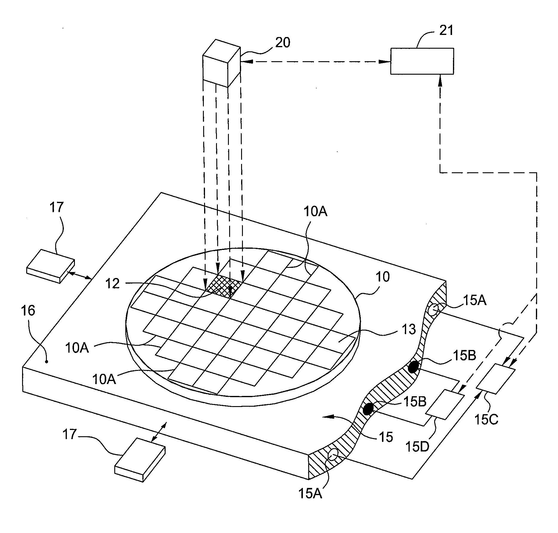
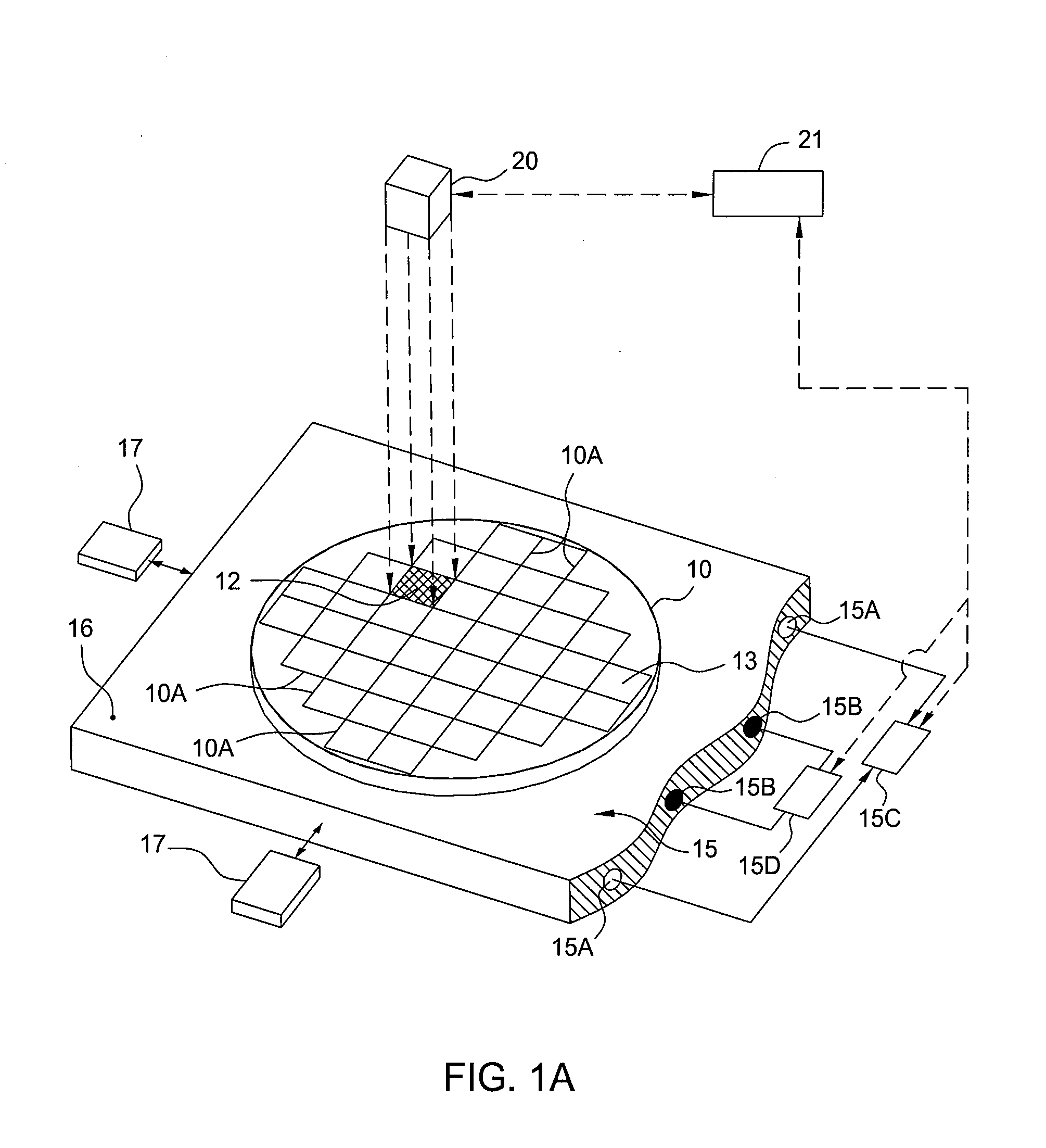
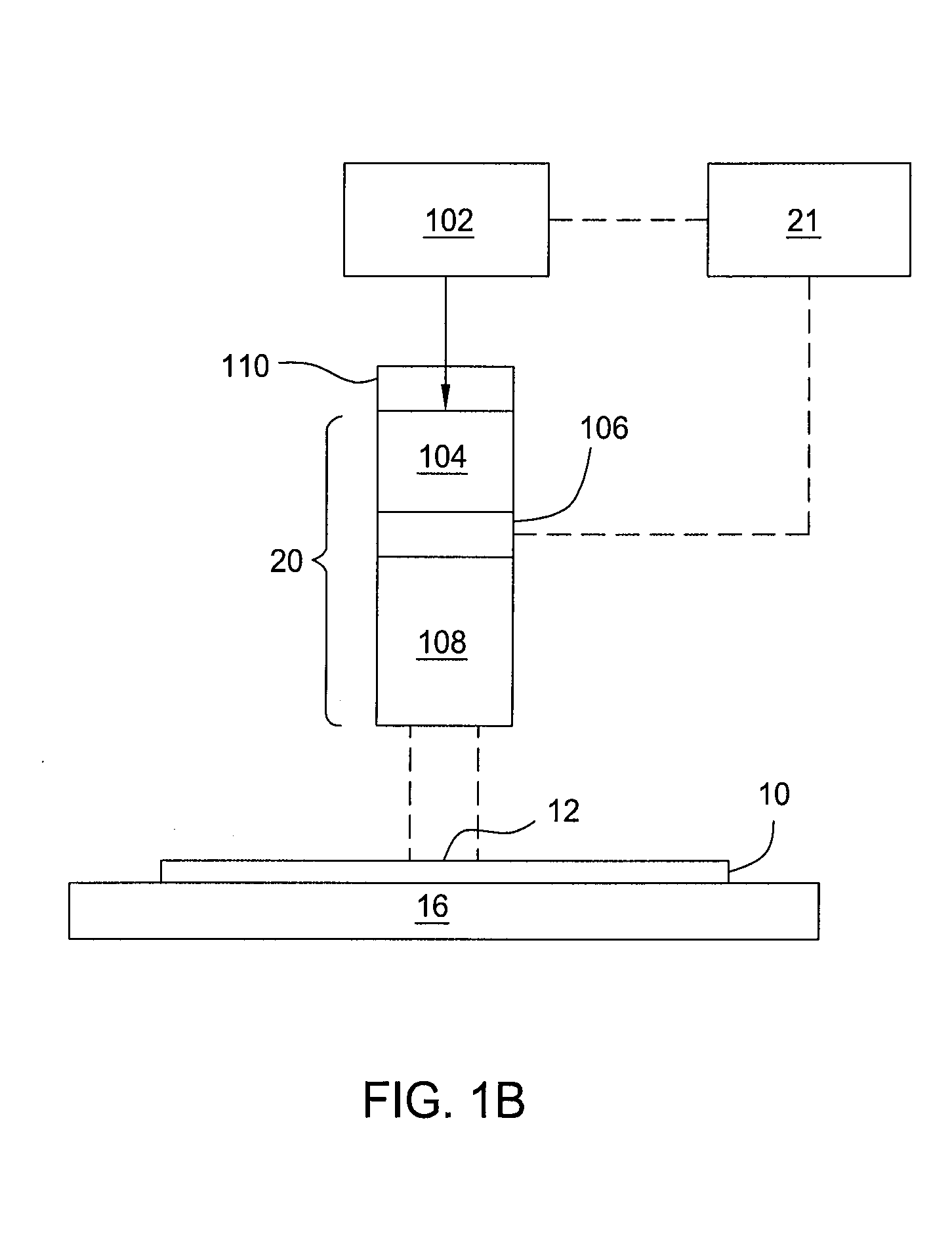
[0107]PTA treatment of a 200 Angstrom junction layer would be expected to yield useful results. After implanting with a dose of 1015 dopant atoms at an energy of 250 eV, 1000 pulses of 532 nm laser light may be delivered in a train of pulses. With each pulse delivering an energy density of 0.3 J / cm2, duration of about 1 msec, and separated by a rest duration of 30 msec, sheet resistivity of the junction after annealing is expected to be less than about 400 Ω / cm2. The same instance with implant energy of 500 eV is expected to achieve sheet resistivity after annealing generally less than 200 Ω / cm2.

[0108]For example, after implanting with a dose of 2×10¹⁵ boron atoms from an octadecaborane precursor at an energy of 250 eV, PTA treatment was performed with 30 20-nsec. pulses of 532 nm laser light delivered to a substrate at 5 pulses per second, each pulse carrying approximately 150 millijoules (mJ) of energy at a density of 0.234 J / cm2, resulting in resistivity of 537 Ω / cm2 following PT...


PUM

PropertyMeasurementUnit
poweraaaaaaaaaa
peak temperatureaaaaaaaaaa
temperatureaaaaaaaaaa

Abstract

The present invention generally describes apparatuses and methods used to perform an annealing process on desired regions of a substrate. In one embodiment, pulses of electromagnetic energy are delivered to a substrate using a flash lamp or laser apparatus. The pulses may be from about 1 nsec to about 10 msec long, and each pulse has less energy than that required to melt the substrate material. The interval between pulses is generally long enough to allow the energy imparted by each pulse to dissipate completely. Thus, each pulse completes a micro-anneal cycle. The pulses may be delivered to the entire substrate at once, or to portions of the substrate at a time. Further embodiments provide an apparatus for powering a radiation assembly, and apparatuses for detecting the effect of pulses on a substrate.

Description

CROSS-REFERENCE TO RELATED APPLICATIONS[0001]This application is a continuation-in-part of co-pending U.S. patent application Ser. No. 12 / 173,967, filed Jul. 16, 2008, which claims benefit of U.S. Provisional Patent Application Ser. No. 60 / 986,550, filed Nov. 8, 2007. Each of the aforementioned related patent applications is herein incorporated by reference.FIELD OF THE INVENTION[0002]Embodiments of the present invention generally relate to a method of manufacturing a semiconductor device. More particularly, the invention is directed to a method of thermally processing a substrate.BACKGROUND[0003]The market for semiconductor devices continues to follow the path of Moore's Law. Current device geometry of 45 nanometers (nm) is projected to shrink to 20 nm and beyond to meet future performance requirements. For such scaling to be realized, engineering of doped source and drain junctions must focus on placement and movement of single atoms within a very small crystal lattice. For exampl...

Claims


Application Information

Patent Timeline
Patent Type & Authority Applications(United States)
IPC IPC(8): F27D11/00
CPCB23K26/0626B23K2201/40H01L21/02667H01L21/26506H01L21/2686H01L21/324H01L21/67115H01L29/66575B23K26/0066H01L21/268B23K2101/40H01L21/2658H01L21/02B23K26/352
Inventor MOFFATT, STEPHENRANISH, JOSEPH M.
Owner APPLIED MATERIALS INC
Why Eureka
Try Eureka