Latch circuit and flip-flop circuit

a latch circuit and flip-flop technology, applied in the field of latch circuits and flip-flop circuits, can solve the problems of inability to suppress soft errors, inability to cause soft errors, so as to reduce the rate of soft errors in latch circuits and suppress soft errors

Inactive Publication Date: 2009-05-14
NEC ELECTRONICS CORP
View PDF4 Cites 13 Cited by
  • Summary
  • Abstract
  • Description
  • Claims
  • Application Information

AI Technical Summary

Benefits of technology

[0018]According to the present invention, it is possible to reduce a rate of soft error in the latch circuit. Moreover, it is possible to suppress an occurrence of soft error resulting from the charge sharing in the latch circuit.

Problems solved by technology

In recent years, it is known that a soft error is caused by high-energy radiation (alpha ray and neutron beam) irradiating the latch circuit.
The soft error is a transient failure, and if correct data can be rewritten anew, the latch circuit will operate normally again.
In recent years, a problem has been pointed out, of charge sharing that electric charges generated by one time of incidence of radiation are collected by two or more nodes.
As described above, in the conventional technique, it is impossible to suppress the soft error when a plurality of memory nodes collected the electric charges by charge sharing.

Method used


Image

  • Latch circuit and flip-flop circuit
  • Latch circuit and flip-flop circuit
  • Latch circuit and flip-flop circuit

Examples


first embodiment

[0031]FIG. 4 is a circuit diagram showing a configuration of a latch circuit 10 according to a first embodiment of the present invention. The latch circuit 10 in the first embodiment is provided with three or more nodes N1A, N1C, N1E, and N1G as first nodes in which a voltage in a first signal level is set and three or more nodes N2B, N2D, N2F, and N2H as second nodes in which a voltage in a second signal level obtained by inverting the first signal level is set. For example, when a data “1” is set in the nodes N1A, N1C, N1E, and N1G, a data “0” obtained by inverting the data “1” is set in the nodes N2B, N2D, N2F, and N2H. Here, transfer gates (not illustrated) are connected to the nodes N1A, N1C, N1E, and N1G as the first nodes and receive a data to be latched by the latch circuit through the nodes N1A, N1C, N1E, and N1G. Further, transfer gates may be connected between the nodes N1A, N1C, N1E, and N1G as the first nodes and the nodes N2B, N2D, N2F and N2H as the second nodes. Here...

second embodiment

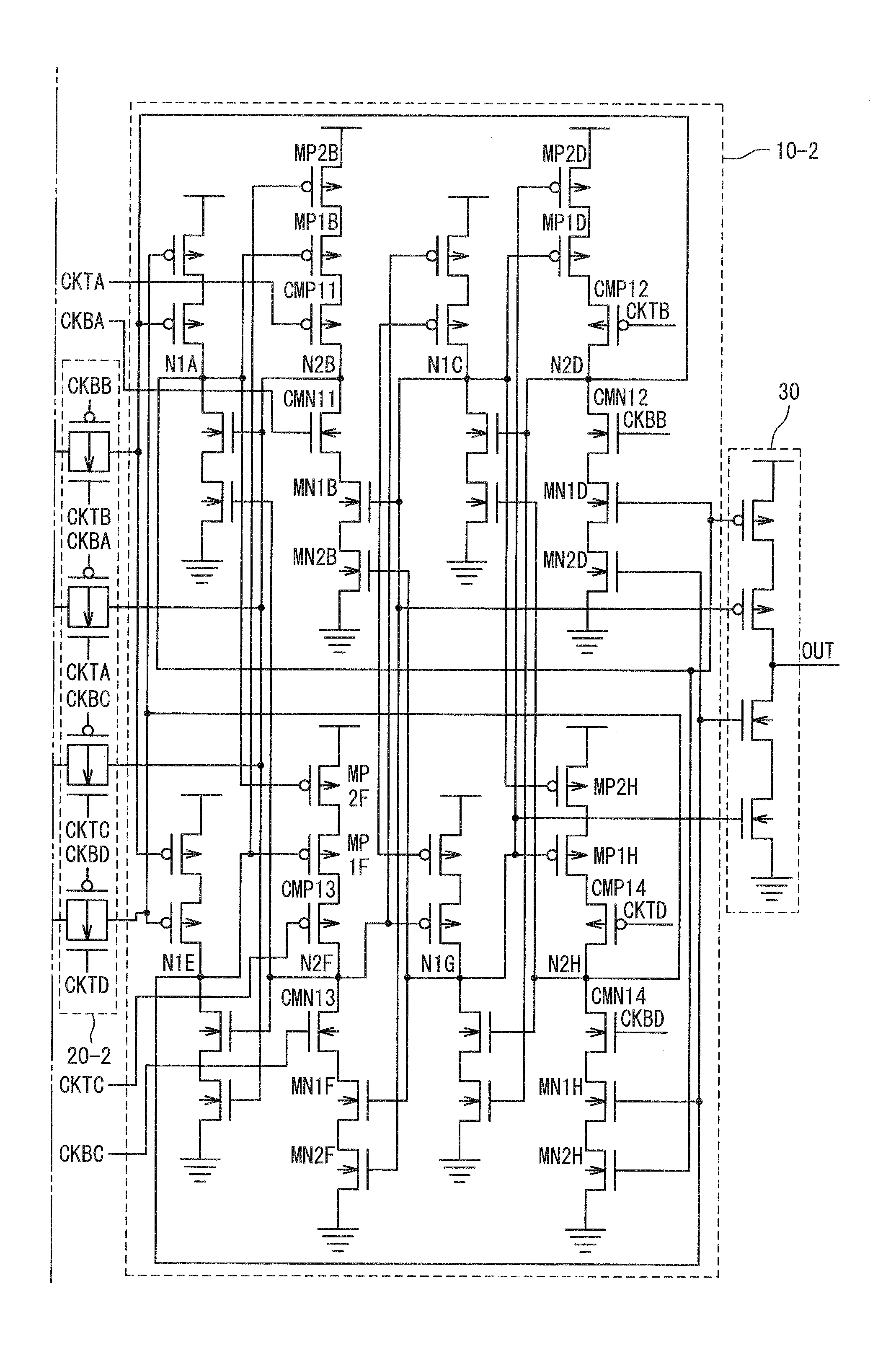
[0065]The latch circuit 10 shown in FIG. 4 may be altered in a part of its configuration. For example, any of the P-channel type MOS transistors MP1A to the N-channel type MOS transistor MN2H for suppressing the voltage value of the data holding node may be removed from the latch circuit 10 shown in FIG. 4. FIG. 6 is a circuit diagram showing the latch circuit 10 according to a second embodiment of the present invention. In the latch circuit 10 shown in FIG. 6, the P-channel type NOS transistors MP2B, MP2D, MP2F, and MP2H and the N-channel type MOS transistors MN2B, MN2D, MN2F, and MN2H are removed from the configuration of the latch circuit 10 shown in FIG. 4.

[0066]Since the transistors with smaller influence of the noise signal are removed in the latch circuit 10 shown in FIG. 6, the latch circuit 10 has an effect of a reduced circuit area although it has a higher generation rate of soft error than the circuit shown in FIG. 4. It is effective to use the circuit shown in FIG. 6 ins...

third embodiment

[0067]Moreover, any one of the node voltage control circuits 1A to 1H may be reduced from the latch circuit 10 shown in FIG. 4. FIG. 7 is a circuit diagram showing the configuration of the latch circuit 10 according to a third embodiment of the present invention. In the latch circuit 10 shown in FIG. 7, the node voltage control circuits 1G and 1H are removed from the latch circuit 10 shown in FIG. 4. The gates of the P-channel type MOS transistors MP2D and the N-channel type MOS transistors MN2B and MN1F are connected to the node N1E, and gates of the P-channel type MOS transistors MP2A and MP1E and the N-channel type MOS transistor MN2C are connected to the node N2C.

[0068]Since in the latch circuit 10 shown in FIG. 7 transistors are removed that cause less influence of noise and nodes whose voltage variation is small are removed, the generation rate of the soft error increases than the circuit shown in FIG. 4, but has an effect of being able to reduce a circuit area. It is effectiv...


PUM


Abstract

A latch circuit includes: first nodes which are three or more and to which a voltage in a first signal level is set; second nodes which are three or more and to which a voltage in a second signal level obtained by inverting the first signal level is set; and first node voltage control circuits having the first nodes; and second node voltage control circuits having the second nodes. Each of the first node voltage control circuits is connected with at least two of the three or more second nodes, and controls the voltage of the first node based on the voltages of the at least two second modes. Each of the second node voltage control circuits is connected with at least two of the three or more first nodes and controls the voltage of the second node based on the voltages of the at least two first nodes.

Description

INCORPORATION BY REFERENCE[0001]This patent application claims priority on convention based on Japanese Patent Application No. 2007-291060. The disclosure thereof is incorporated herein by reference.BACKGROUND OF THE INVENTION[0002]1. Field of the Invention[0003]The present invention relates to a latch circuit and a flip-flop circuit that uses it.[0004]2. Description of Related Art[0005]In recent years, it is known that a soft error is caused by high-energy radiation (alpha ray and neutron beam) irradiating the latch circuit. The soft error is a failure caused by “singe-event upset (SEU)” in which data is inverted, resulting from a phenomenon that alpha rays and / or neutron beams are incident on the latch circuit to generate electric charges and the electric charges are collected by a region (node) for retaining the data. The soft error is a transient failure, and if correct data can be rewritten anew, the latch circuit will operate normally again. However, even if it is temporary, s...

Claims


Application Information

Patent Timeline
Patent Type & Authority Applications(United States)
IPC IPC(8): H03K3/356H03K3/00
CPCH03K3/356191H03K3/0375
Inventor YAMAMOTO, HIROSHI
Owner NEC ELECTRONICS CORP
Why Eureka
Try Eureka