Method of fabricating a semiconductor device having a photo-sensitive polyimide layer and a device fabricated in accordance with the method

a polyimide layer and semiconductor technology, applied in the field of manufacturing a semiconductor device having a photosensitive polyimide layer and a device fabricated in accordance with the method, can solve the problems of higher probability of cracking in the pspl layer, unfavorable underlying pspl layer development, so as to reduce the device soft error rate (ser) and avoid unwanted development of the underlying

Inactive Publication Date: 2005-02-10
SAMSUNG ELECTRONICS CO LTD
View PDF1 Cites 1 Cited by
  • Summary
  • Abstract
  • Description
  • Claims
  • Application Information

AI Technical Summary

Benefits of technology

[0012] The present invention is directed to a method and product formed in accordance with the method in which a PSPL layer is used in the fabrication of a semiconductor device in a manner which overcomes the limitations of the conventional approaches. The beneficial qualities of an added photoresist layer are utilized to avoid unwanted development of the underlying PSPL layer. In this manner, cracking of the PSPL layer is mitigated or eliminated, reducing the device soft error rate (SER) and increasing device yield. This is accomplished in a reliable and low-cost approach that employs standard device fabrication techniques.

Problems solved by technology

However, such EMC configurations are known to be a source of mechanical stress that is incident on the chips.
However, during exposure, a portion of the light can stray to improperly irradiate other regions of the PSPL, leading to unwanted exposure regions 19a in other locations of the structure.
This results in a higher likelihood of cracking in the PSPL layer, which corresponds directly with an increase in the device soft error rate (SER).
Lengthening of exposure time and increase in the exposure energy can cause a degradation of process throughput and increase the likelihood of pad open failure in the subsequent etching process.
In addition, since the photoresist pattern is removed only after exposing the underlying bonding pad, it is difficult to remove the relatively thick photoresist pattern without causing damage to the underlying PSPL and the exposed pad during the removal process.

Method used


Image

  • Method of fabricating a semiconductor device having a photo-sensitive polyimide layer and a device fabricated in accordance with the method
  • Method of fabricating a semiconductor device having a photo-sensitive polyimide layer and a device fabricated in accordance with the method
  • Method of fabricating a semiconductor device having a photo-sensitive polyimide layer and a device fabricated in accordance with the method

Examples


Embodiment Construction

[0027] In the following description of preferred embodiments of the present invention and in the claims that follow, the term “on”, when referring to layers of material used in the fabrication of the semiconductor devices, refers to a layer that is directly applied to an underlying layer, or refers to a layer that is above an underlying layer with an optional intermediate layer or layers therebetween.

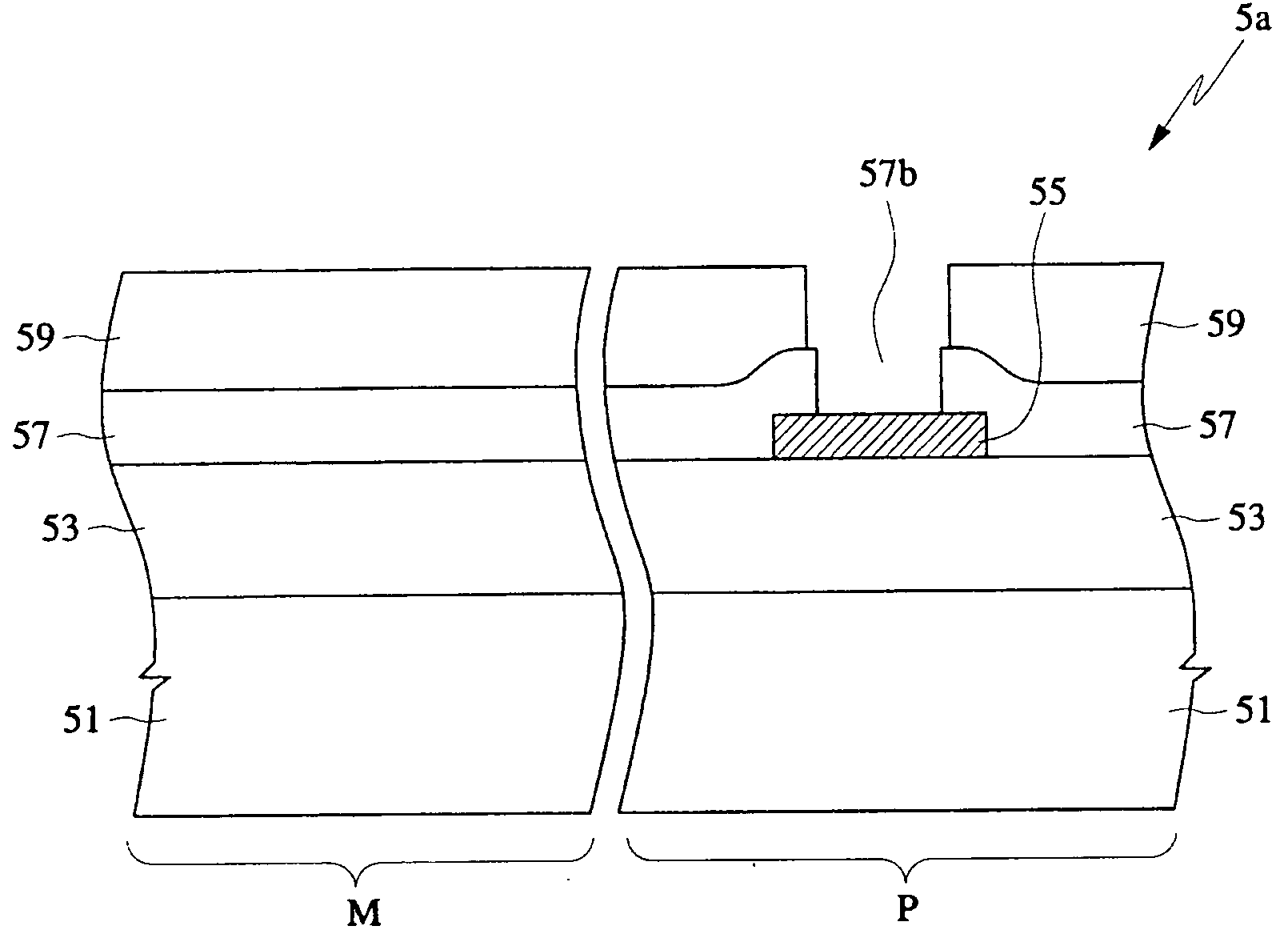
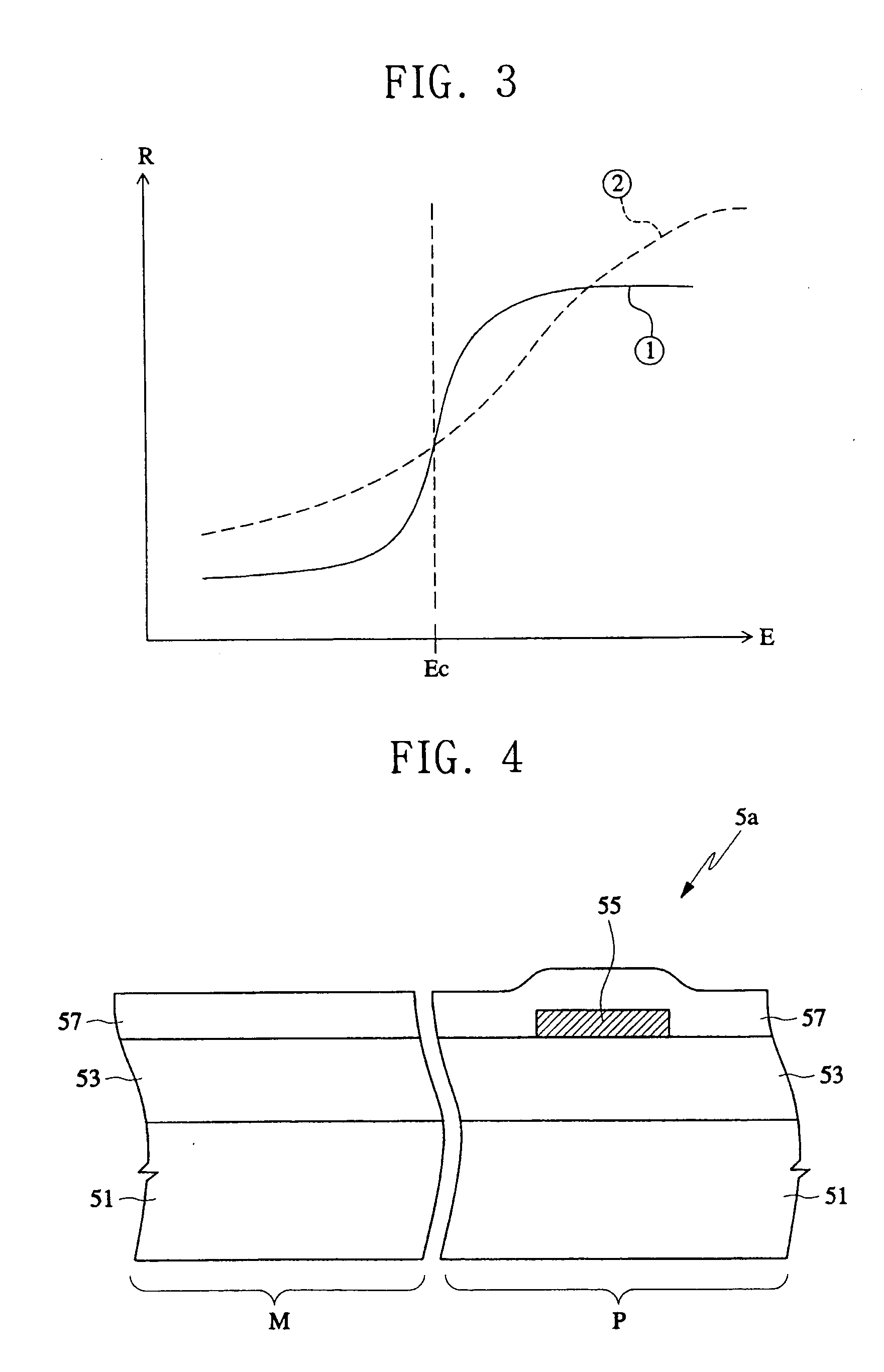
[0028]FIGS. 4-7 are cross-sectional views of a fabrication method for forming a semiconductor device utilizing a PSPL, in accordance with the present invention. As in the above figures, M represents an internal circuit region of a device, and P represents a bonding pad region of a device. Although the present invention is described in conjunction with using a PSPL layer to form a via hole for exposing a bonding pad region, the present invention applies equally well to using a PSPL layer in other fabrication processes, as well as use of a PSPL layer in conjunction with other components ...


PUM


Abstract

In a semiconductor device fabrication method and in a product formed according to the method, a photosensitive polyimide layer (PSPL) layer is applied to a semiconductor device in a manner which overcomes the limitations of the conventional approaches. The beneficial qualities of an added photoresist layer are utilized to avoid unwanted development of the underlying PSPL layer. In this manner, cracking of the PSPL layer is mitigated or eliminated, reducing the device soft error rate (SER) and increasing device yield. This is accomplished in a reliable and low-cost approach that employs standard device fabrication techniques.

Description

BACKGROUND OF THE INVENTION [0001] Semiconductor devices formed on a substrate, commonly referred to as “chips”, are often times encapsulated during the assembly process in order to protect the devices from external environmental influences. For example, during assembly, the chips are commonly coated with an epoxy molding compound (EMC), which serves as a physical barrier for the chip. However, such EMC configurations are known to be a source of mechanical stress that is incident on the chips. For this reason, prior to formation of the EMC, the upper surface of a chip is covered with a polyimide layer during fabrication, which serves to alleviate the mechanical stress. [0002] The polyimide layer further serves to prevent nearby energized particles from entering the chip, which could have an adverse effect on data stored in the chip, or otherwise affect chip operation. For example, the polyimide layer prevents alpha particles from penetrating the chip devices, thereby reducing the so...

Claims


Application Information

Patent Timeline
Patent Type & Authority Applications(United States)
IPC IPC(8): H01L21/312H01L21/027H01L23/31
CPCH01L21/0271H01L21/0274H01L21/312H01L23/3192H01L2924/0002H01L2924/19041H01L2924/00H01L21/02118G03F7/0045G03F7/2002H01L21/0273
Inventor KIM, JAE-HYUNSHIN, DONG-WONKIM, BOO-DEUKLEE, CHANG-HOKIM, WON-MIPARK, SEOK-BONG
Owner SAMSUNG ELECTRONICS CO LTD
Why Eureka
Try Eureka