Semiconductor device

a technology of semiconductor devices and semiconductors, applied in semiconductor devices, semiconductor/solid-state device details, electrical apparatus, etc., can solve the problems of increasing the thickness of the semiconductor device, increasing manufacturing costs, etc., and achieve the effect of preventing crack formation in the passivation film and increasing the thickness

Active Publication Date: 2009-05-21
ROHM CO LTD
View PDF23 Cites 3 Cited by
  • Summary
  • Abstract
  • Description
  • Claims
  • Application Information

AI Technical Summary

Benefits of technology

[0011]An object of the present invention is to provide a semiconductor device with which crack formation in a passivation film can be prevented without causing increase in number of manufacturing steps, increase in thickness and other problems.

Problems solved by technology

However, because a step of forming the polyimide layer must be added, a number of manufacturing steps of the semiconductor device 101 is increased and this causes increase in manufacturing cost.
Thus, there is an issue of increase in thickness of the semiconductor device 101.

Method used


Image

  • Semiconductor device
  • Semiconductor device
  • Semiconductor device

Examples


Embodiment Construction

[0028]An embodiment of the present invention shall now be described in detail with reference to the attached drawings.

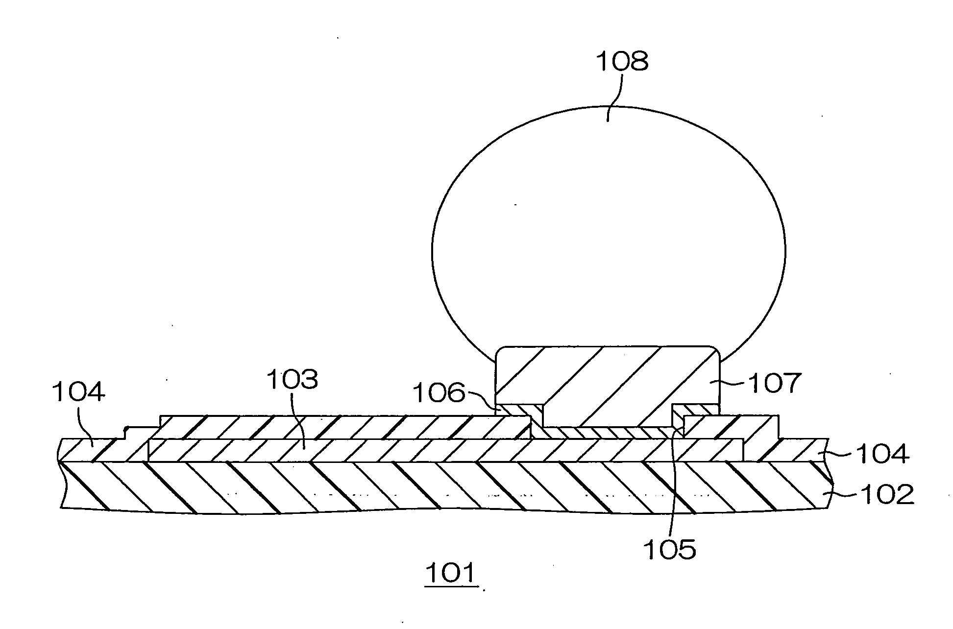
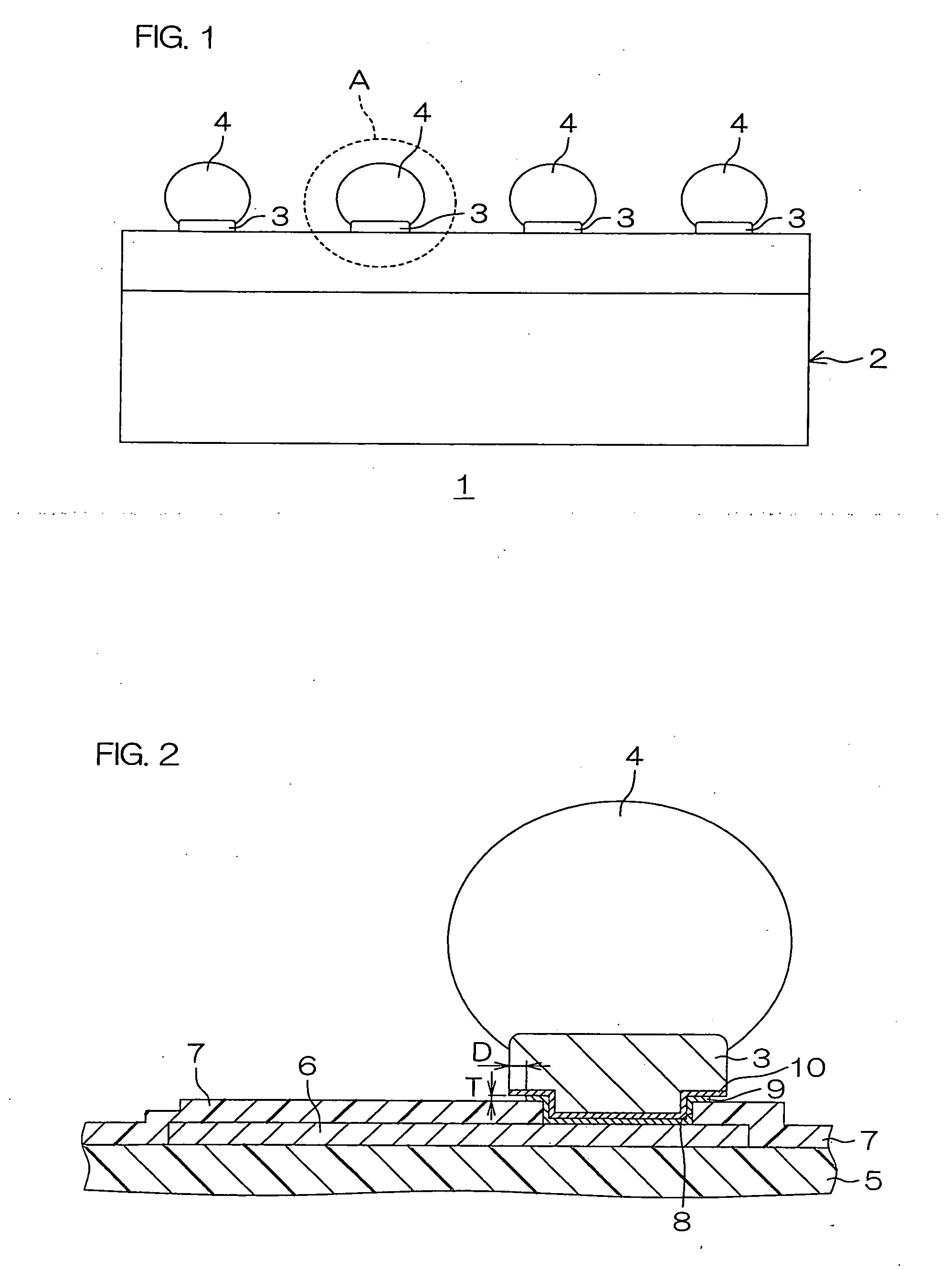
[0029]FIG. 1 is a side view of an outer appearance of a semiconductor device according to a first embodiment of the present invention.

[0030]A WL-CSP technology is applied in the semiconductor device 1. The semiconductor device 1 includes a semiconductor chip 2, a plurality of post bumps 3 disposed on the semiconductor chip 2, and solder balls 4 bonded to the respective post bumps 3.

[0031]FIG. 2 is a schematic sectional view of a structure of a portion surrounded by a broken line A in FIG. 1.

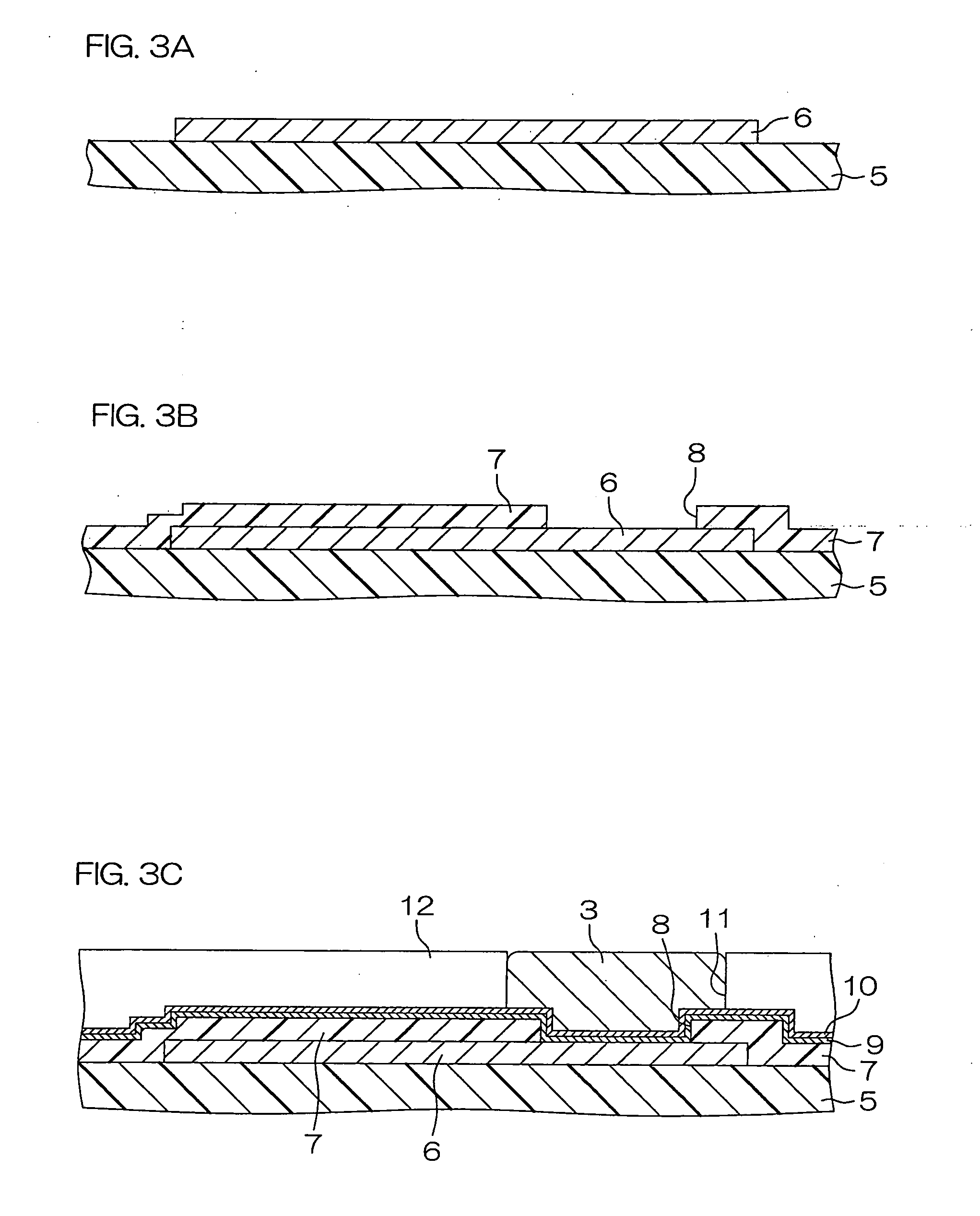
[0032]An interlayer insulating film 5 made of SiO2 is formed on a top layer portion of the semiconductor chip 2. A wiring 6 made of Al is formed in a predetermined pattern on the interlayer insulating film 5.

[0033]A passivation film 7 made of SiN is formed on the interlayer insulating film 5 and the wiring 6. The wiring 6 is covered by the passivation film 7. An opening 8 for expo...


PUM


Abstract

A semiconductor device according to the present invention includes: a semiconductor chip; a wiring formed on the semiconductor chip; a passivation film, coating the wiring and having an opening for partially exposing the wiring from the passivation film; an interposing film, formed on a portion of the wiring facing the opening; and a post bump, raisedly formed on the interposing film and with a peripheral edge portion thereof protruding more toward a side than a peripheral edge of the interposing film.

Description

BACKGROUND OF THE INVENTION[0001]1. Field of the Invention[0002]The present invention relates to a semiconductor device applying a so-called WL-CSP (Wafer Level-Chip Size Package) technology.[0003]2. Description of Related Art[0004]With the recent making of semiconductor devices more advanced in function and multifunctional, practical use of WL-CSP technology is progressing. With a WL-CSP technology, a packaging process is completed in a wafer state, and a size of each individual chip cut out by dicing becomes a package size.[0005]FIG. 4 is a schematic sectional view of a structure of a semiconductor device to which a WL-CSP technology is applied.[0006]The semiconductor device 101 includes a semiconductor chip (not shown) making up a base thereof. An interlayer insulating film 102 made of SiO2 (silicon oxide) is formed on the semiconductor chip. A wiring 103 made of Al (aluminum) is formed in a predetermined wiring pattern on the interlayer insulating film 102. A passivation film 10...

Claims


Application Information

Patent Timeline
Patent Type & Authority Applications(United States)
IPC IPC(8): H01L23/52H01L23/48H01L23/482
CPCH01L23/525H01L24/03H01L2924/0002H01L2224/0401H01L2224/05559H01L2224/05018H01L2924/01074H01L2924/01033H01L2924/01006H01L2924/014H01L2924/01079H01L2924/01078H01L2924/01073H01L24/05H01L24/11H01L24/13H01L2224/0345H01L2224/0361H01L2224/03912H01L2224/03914H01L2224/05017H01L2224/05027H01L2224/05166H01L2224/05541H01L2224/0556H01L2224/05564H01L2224/05572H01L2224/05647H01L2224/1147H01L2224/11912H01L2224/13006H01L2224/13018H01L2224/13022H01L2224/13082H01L2224/131H01L2224/13144H01L2924/01013H01L2924/01029H01L2924/00014H01L2224/05552H01L23/3171H01L23/528H01L24/32H01L2224/1301H01L2224/32501H01L24/08H01L24/09H01L24/14H01L2224/05558H01L2224/05582H01L2224/05666H01L2224/05684
Inventor SAMESHIMA, KATSUMI
Owner ROHM CO LTD
Why Eureka
Try Eureka