This helps you quickly interpret patents by identifying the three key elements:
Problems solved by technology
Method used
Benefits of technology
Benefits of technology
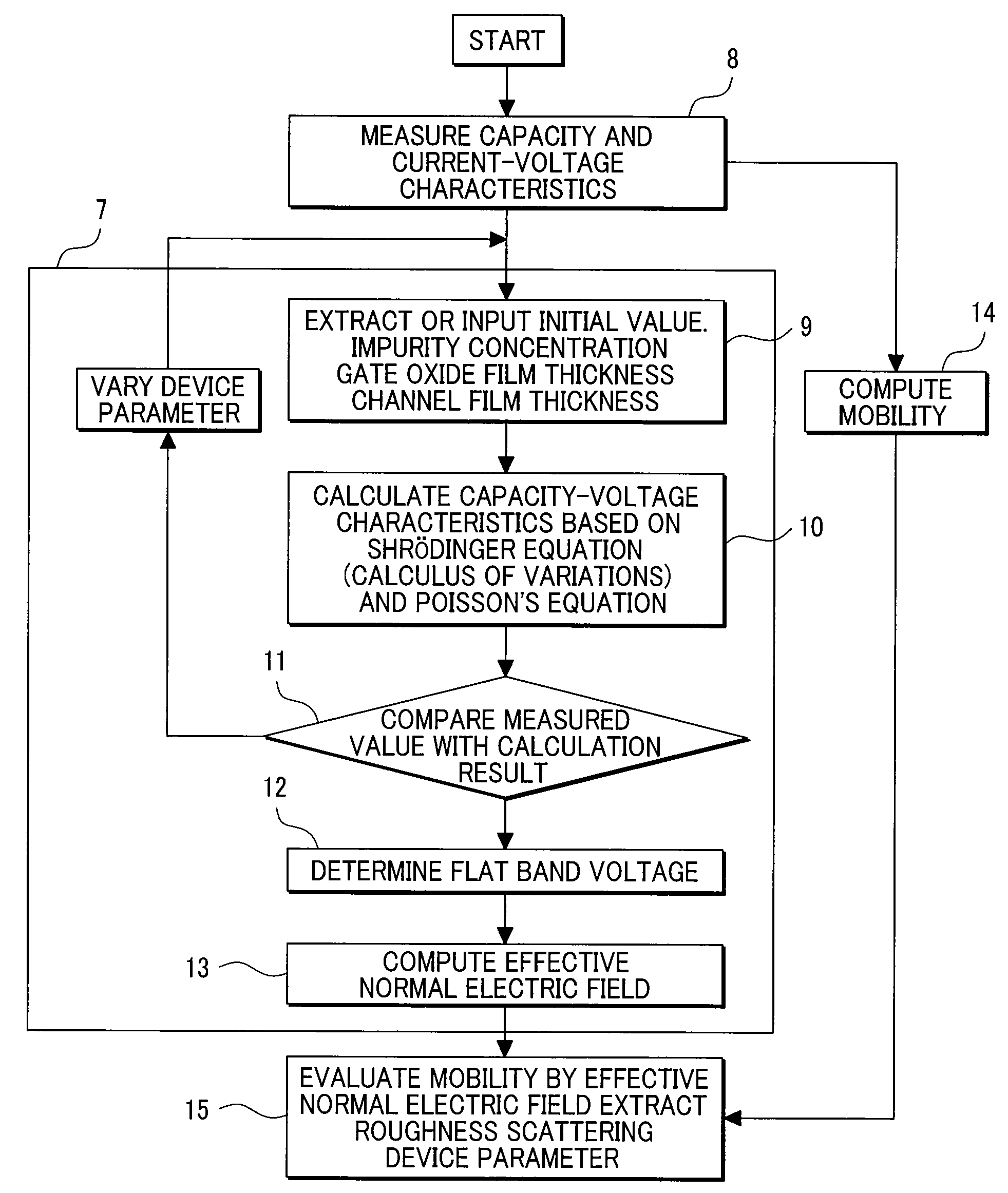
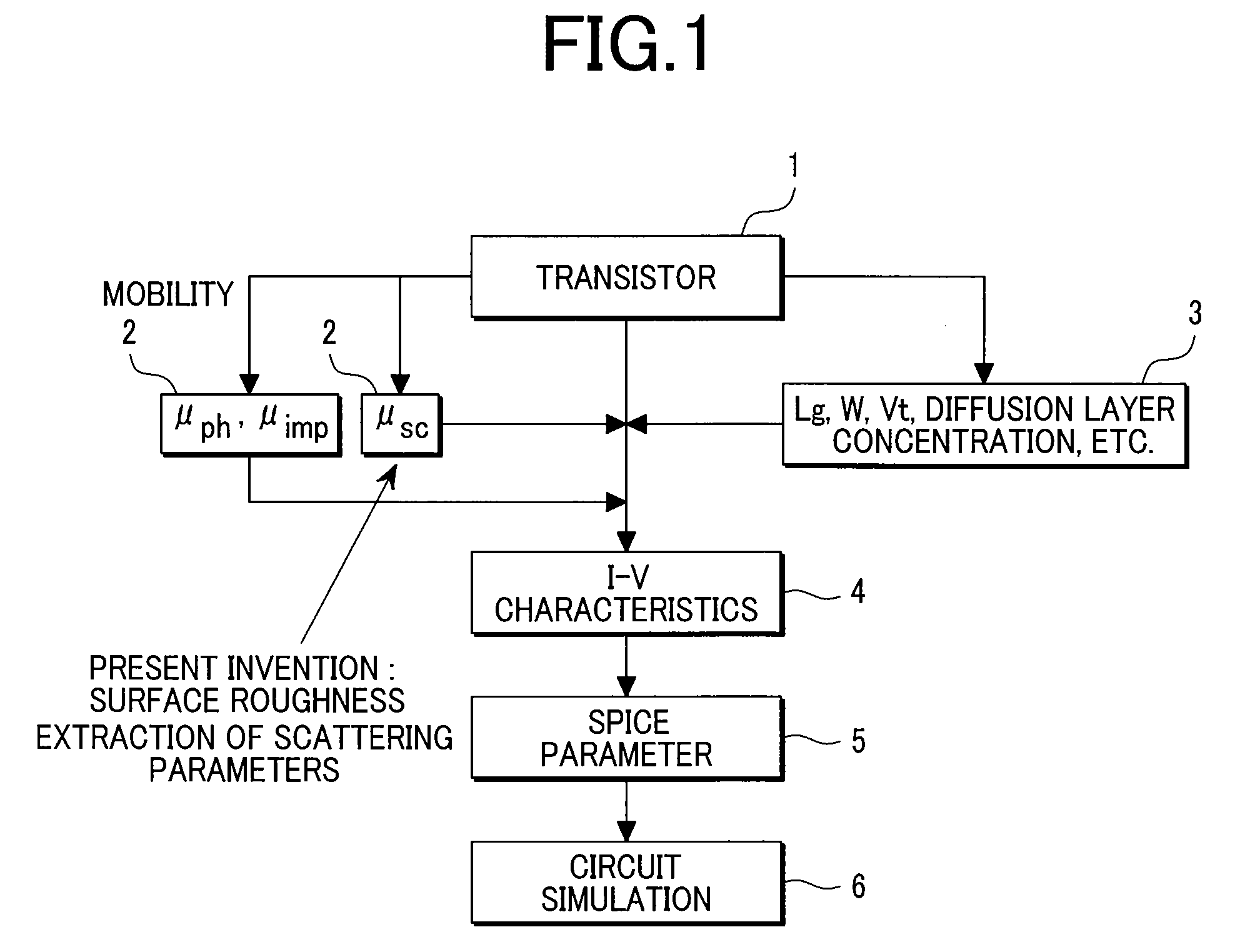
[0067]To briefly explain major benefits of the present invention, it makes it possible to measure the dependency of mobility of a transistor having plural gates on surface roughness scattering. In addition, it enables to extract a device parameter for roughness scattering of a transistor having plural gates. Further, it inputs the extracted device parameter to a circuit simulator. Accordingly, it is now possible to provide a circuit simulator for a circuit device using any industry leading transistor with plural gates.
Problems solved by technology
Since it is customarily impossible to derive an effective normal electric field from a transistor similar to the one shown in FIGS. 5 to 8, which has a plural number of gate electrodes, by adopting the same method used in a bulk transistor, evaluation of the dependency of mobility on the effective normal electric field was somewhat difficult.
Accordingly, no body has yet discovered a method for extracting a roughness scattering device parameter in such a transistor.
First, if a channel section in a transistor with plural gates is isolated by a substrate and an insulating film, holes are not formed so one cannot measure an accumulation-layer capacity.
Second, because there are many gates, if one wants to fix a certain gate voltage and then change another gate voltage or plural gate voltages at the same time, it is not apparent how to perform integrations corresponding to Eq.
Method used
Image
Click on the blue label to locate the original text in one second.
Reading with bidirectional positioning of images and text.
Examples
embodiment 1
[0098]An application of the present invention to an SOTB transistor, a kind of double gate transistors (n=2), will now be explained. FIG. 12 and FIG. 13 respectively illustrate a Silicon On Thin Buried Oxide (abbreviated to as “SOTB”) transistor. This transistor is a kind of Silicon On Insulator transistors where channel and silicon substrate are isolated by an insulation layer, and is characterized in that an insulating film on a back gate electrode side is as thin as 10 nm and that a channel is formed on a front gate side to utilize the back gate for control of V1. Therefore, only an effective normal electric field seen from the front gate side is extracted. Particularly, plane orientation of silicon in a direction normal to a gate is called a (100) plane.
[0099]Suppose that VG1 and Q1 are gate voltage and charge on the front gate side, VG2 and Q2 gate voltage and charge on the back gate side, Q0 channel charge, and Q1inv and Q1acc charge at an inversion layer and an accounting lay...
embodiment 2
[0117]For a transistor like the one shown in FIG. 7, which has three gates and a channel region thereof is in direct contact with a substrate, Fang-Howard variation wave function (Ψ(x)=Axe−λx, (0≦x≦∞) and a calculation method for a bulk transistor are applied, given that a voltage is impressed to a gate 16a of FIG. 7. On the other hand, if a voltage is impressed to a gate 16b, calculation methods explained in Eq. (46) and Eq. (47) for a double gate transistor are applied. In result, an equation for a current-voltage curve is obtained identically to Embodiment 1, and an operation waveform of a ring oscillator 51's inverters was reproduced.
embodiment 3
[0118]For a transistor having four gates like the one shown in FIG. 8, calculation methods explained in Eq. (46) and Eq. (47) for a double gate transistor are applied, provided that only voltage between two opposite gates is varied, and a flat band voltage is applied to the other gates. In addition, in case of applying voltages to four gates simultaneously, a wave function may be written as follows, obeying in Eq. (29):
where tsi1 and tsi2 stand for distances between two opposite gates. Other parameters have the same meaning as those in Eq. (29). Substituting Eq. (17) into the following formula yields capacity at a j-th gate (j=0, 1, 2, 3, 4) or a channel:
[0119]In result, an equation for a current-voltage curve is obtained identically to Embodiment 1, and an operation w...
PUM
Abstract
Capacity-gate voltage characteristics of a field-effect transistor having plural gates are measured against a voltage change in each one of the gates for an inverted MOSFET and for an accumulated MOSFET, respectively. These measurements together with numerical simulations provided from a model for quantum effects are used to determine flat band voltages between the plural gates and a channel. Next, an effective normal electric field is calculated as a vector line integral by using a set of flat band voltages for the measured capacity as a lower integration limit. Lastly, mobility depending on the effective normal electric field is calculated from current-gate voltage characteristic measurements and capacity measurements in a source-drain path, and the calculated mobility is substituted into an equation for a current-voltage curve between source and drain.
Description
CLAIM OF PRIORITY[0001]The present application claims priority from Japanese application JP 2007-301276, filed on Nov. 21, 2007, the content of which is hereby incorporated by reference into this application.BACKGROUND OF THE INVENTION[0002]1. Field of the Invention[0003]The present invention relates in general to a design method for a semiconductor circuit, more specifically, to a design method for a semiconductor circuit characterized by a field-effect transistor having plural gate electrodes to extract characteristics of a circuit which the transistor is mounted on.[0004]2. Background of the Related Arts[0005]In development of semiconductor devices such as LSIs, circuit simulation is an important process to achieve a shortened development period by predicting characteristics of a circuit prior to prototype production. In a traditional standard circuit simulation, current-voltage characteristics of a transistor, a primary circuit-constituent element, have been described in use of ...
Claims
Application Information
Patent Timeline
Application Date:The date an application was filed.
Publication Date:The date a patent or application was officially published.
First Publication Date:The earliest publication date of a patent with the same application number.
Issue Date:Publication date of the patent grant document.
PCT Entry Date:The Entry date of PCT National Phase.
Estimated Expiry Date:The statutory expiry date of a patent right according to the Patent Law, and it is the longest term of protection that the patent right can achieve without the termination of the patent right due to other reasons(Term extension factor has been taken into account ).
Invalid Date:Actual expiry date is based on effective date or publication date of legal transaction data of invalid patent.

