Si-polymers and photoresists comprising same
a technology of photoresists and polymers, applied in the direction of photosensitive materials, auxillary/base layers of photosensitive materials, instruments, etc., can solve the problems of increasing the resist thickness over diffusion steps on a substrate and into etched patterns, and reducing the quality of electronic packages. , to achieve the effect of sufficient solubility differentials
- Summary
- Abstract
- Description
- Claims
- Application Information
AI Technical Summary
Benefits of technology
Problems solved by technology
Method used
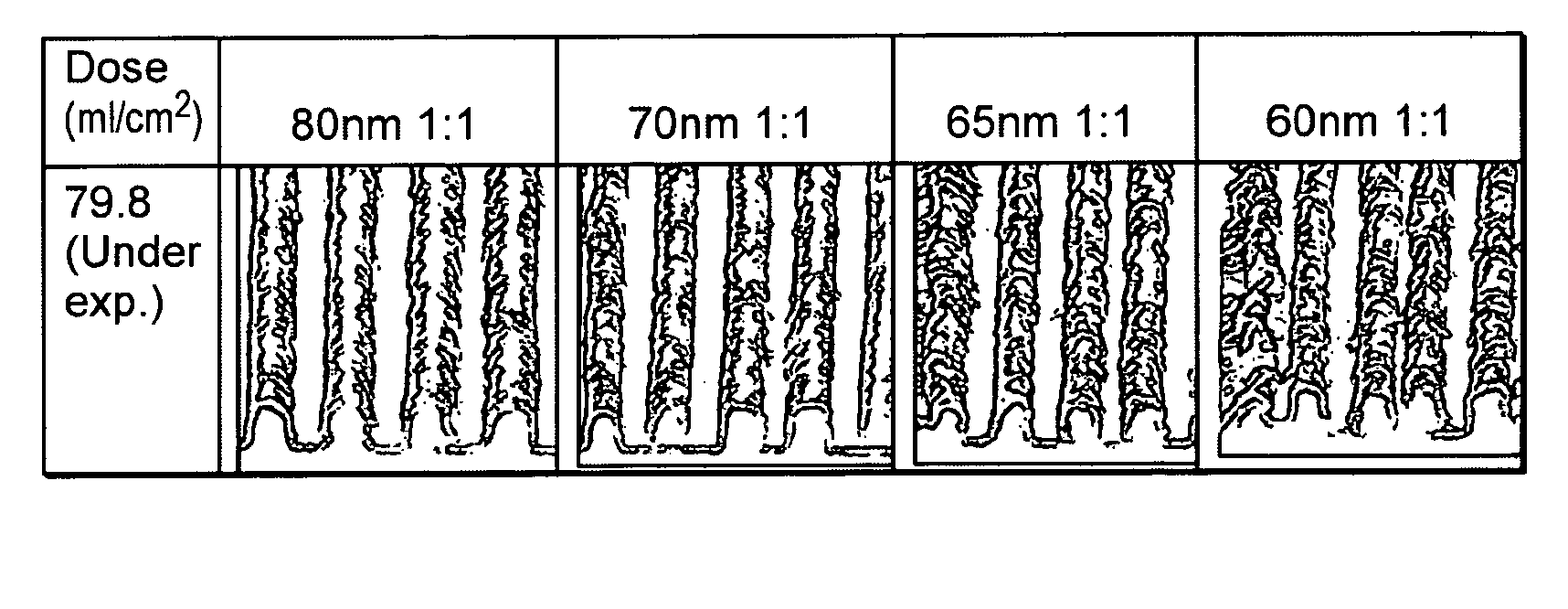
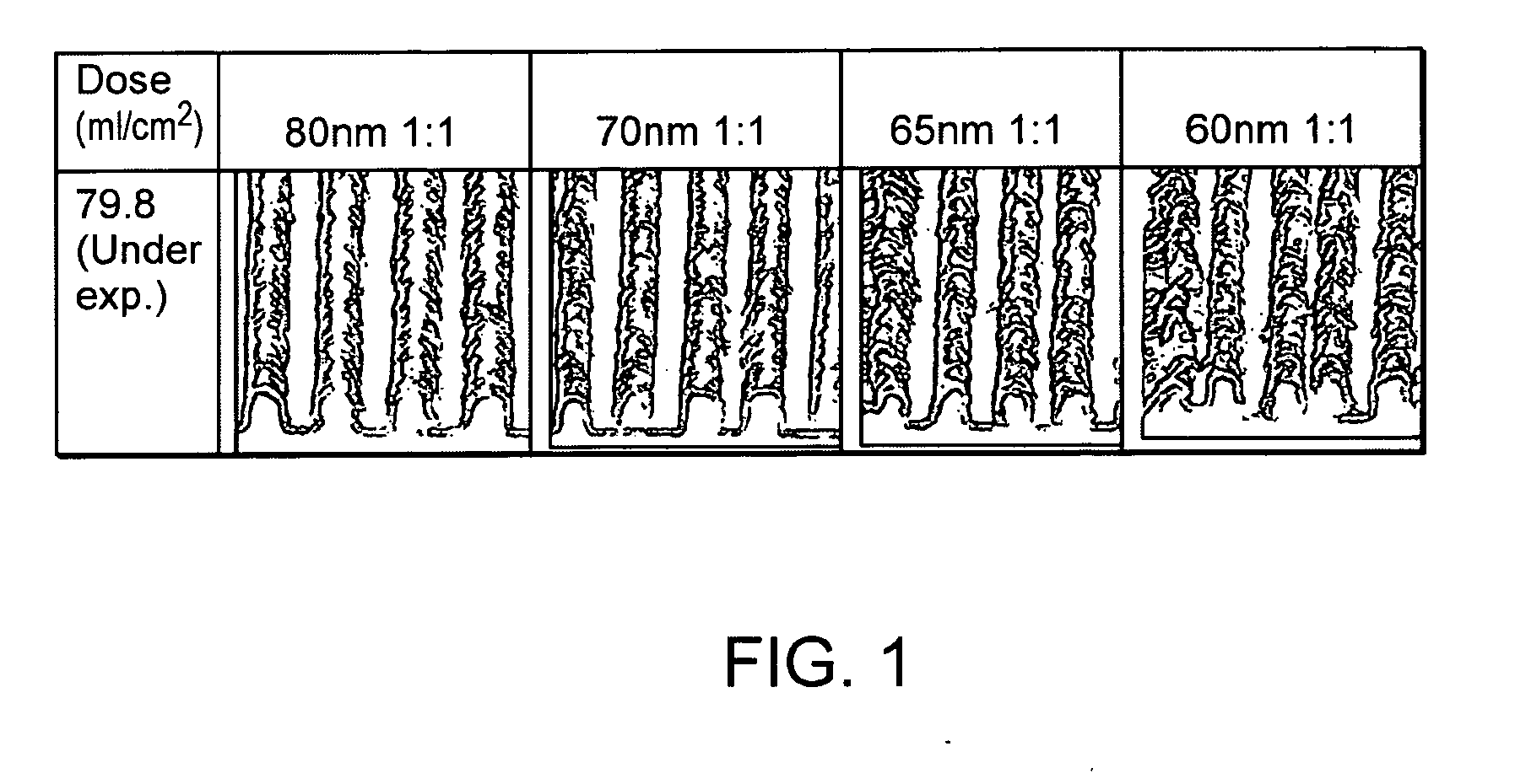
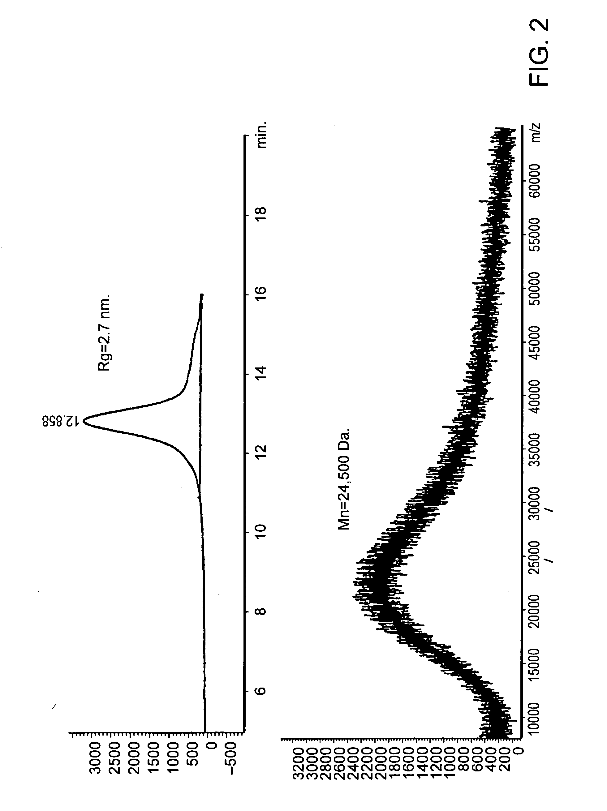
Image

Examples
examples 1-5
Syntheses of Monomers Useful for Preparation of Polymers of the Invention
example 1
Synthesis of 1,1,1-trifluoro-2-trifluoromethyl-pent-4-en-2-ol (BTHB)-triethoxysilane
[0132]
[0133]Part 1. To 10 g of 1,1,1-trifluoro-2-trifluoromethyl-pent-4-en-2-ol (48 mmol) dissolved in 30 ml of anhydrous toluene were added 7.2 g of trichlorosilane (53 mmol) and 5 drops of Karstedt's catalyst solution. The reaction mixture was heated to reflux and while stirred with a magnetic stirring bar was kept at reflux overnight. After this period of reaction the solvent and the other volatiles components present in the product mixture were remover under reduced pressure. 1H NMR spectroscopy of the residue showed that the formation of the trichlorosilane intermediate had proceeded to completion. The product was then used to form polymers of the invention or the triethoxysilane monomer without further purification.
[0134]Part 2. 16 g of 1,1,1-trifluoro-2-trifluoromethyl-pent-4-en-2-ol (BTHB)-trichlorosilane (46 mmol) prepared according to the above procedure was added to a 100 ml flask equipped...
example 2
Synthesis of hexafluoroisopropylnorbornyl(HFIPNB)-triethoxysilane
[0135]
[0136]The syntheses of HFIPNB-trichlorosilane and HFIPNB-triethoxysilane are the same as those of BTHB-trichlorosilane and of BTHB-triethoxysilane as set forth in Example 1 above. The tricholorosilane intermediate was used to form polymers of the invention or converted as shown in the equation to the triethoxysilane monomer. The final triethoxysilane monomer was collected at 150° C. / 6 mmHg.
PUM
| Property | Measurement | Unit |
|---|---|---|
| wavelengths | aaaaa | aaaaa |
| wavelengths | aaaaa | aaaaa |
| wavelengths | aaaaa | aaaaa |
Abstract
Description
Claims
Application Information
 - R&D Engineer
- R&D Manager
- IP Professional
- Industry Leading Data Capabilities
- Powerful AI technology
- Patent DNA Extraction
Browse by: Latest US Patents, China's latest patents, Technical Efficacy Thesaurus, Application Domain, Technology Topic.
© 2024 PatSnap. All rights reserved.Legal|Privacy policy|Modern Slavery Act Transparency Statement|Sitemap