Light emitting unit

a technology of light-emitting units and light-emitting components, which is applied in the direction of semiconductor devices for light sources, light-emitting devices, and planar light sources, can solve the problems that the conventional structure cannot solve the heat dissipation problem, and achieve the effects of enhancing heat dissipation effect, high thickness, and large area

Inactive Publication Date: 2009-06-04
GIGNO TECH CO LTD
View PDF12 Cites 162 Cited by
  • Summary
  • Abstract
  • Description
  • Claims
  • Application Information

AI Technical Summary

Benefits of technology

[0013]As mentioned above, since the light emitting unit of the present invention allows the LED die to dispose in a chamber, the light emitting unit no longer needs a molding compound with a large area and high thickness to entirely cover the LED dies. Without separation from the molding compound, the heat can be dissipated from the substrate below the LED die and also from the top of the LED die. Meanwhile, the heat dissipation effect can be enhanced by the heat convection effect of the gel or the fluid, and the deformation or the breaking of the wire connected between the LED die and the substrate caused by dragging and squeezing can be avoided. In addition, the LED die can be protected from the moisture, dust, or other environmental factors by the housing. Moreover, the light emitting unit of the present invention still can use the molding compound, which partially covers a single LED die, for enhancing the light extraction efficiency and the light emission range of the LED die.

Problems solved by technology

Additionally, the conventional structure cannot solve the heat dissipation problem of the LED die 12.

Method used


Image

  • Light emitting unit
  • Light emitting unit
  • Light emitting unit

Examples


first embodiment

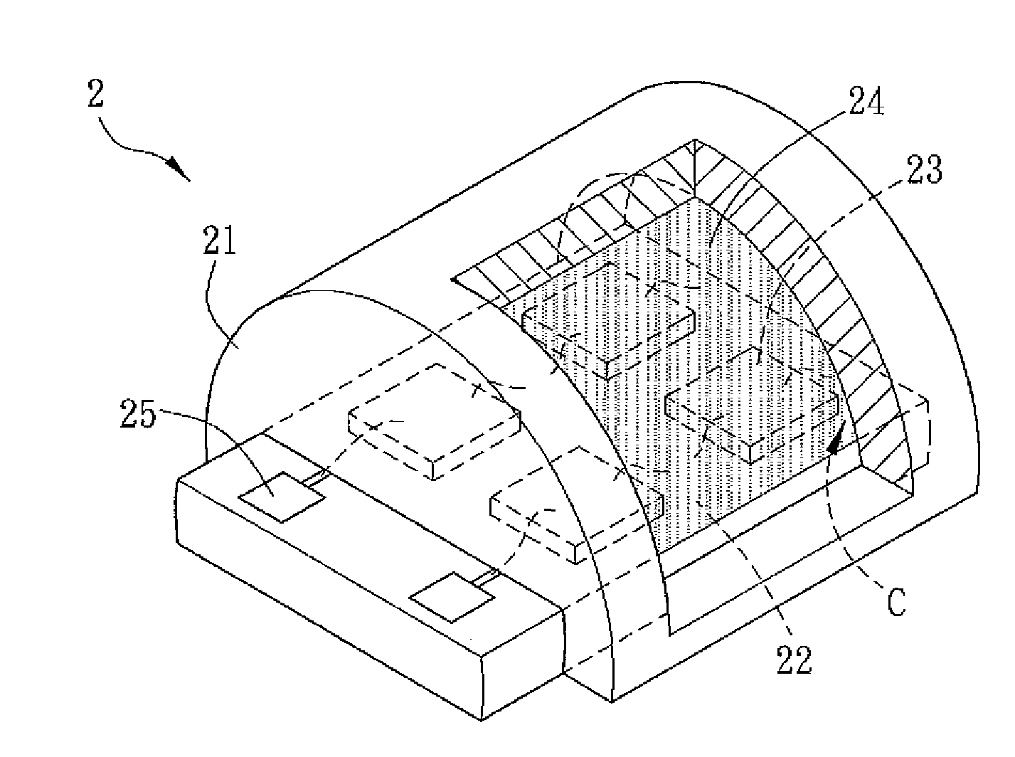
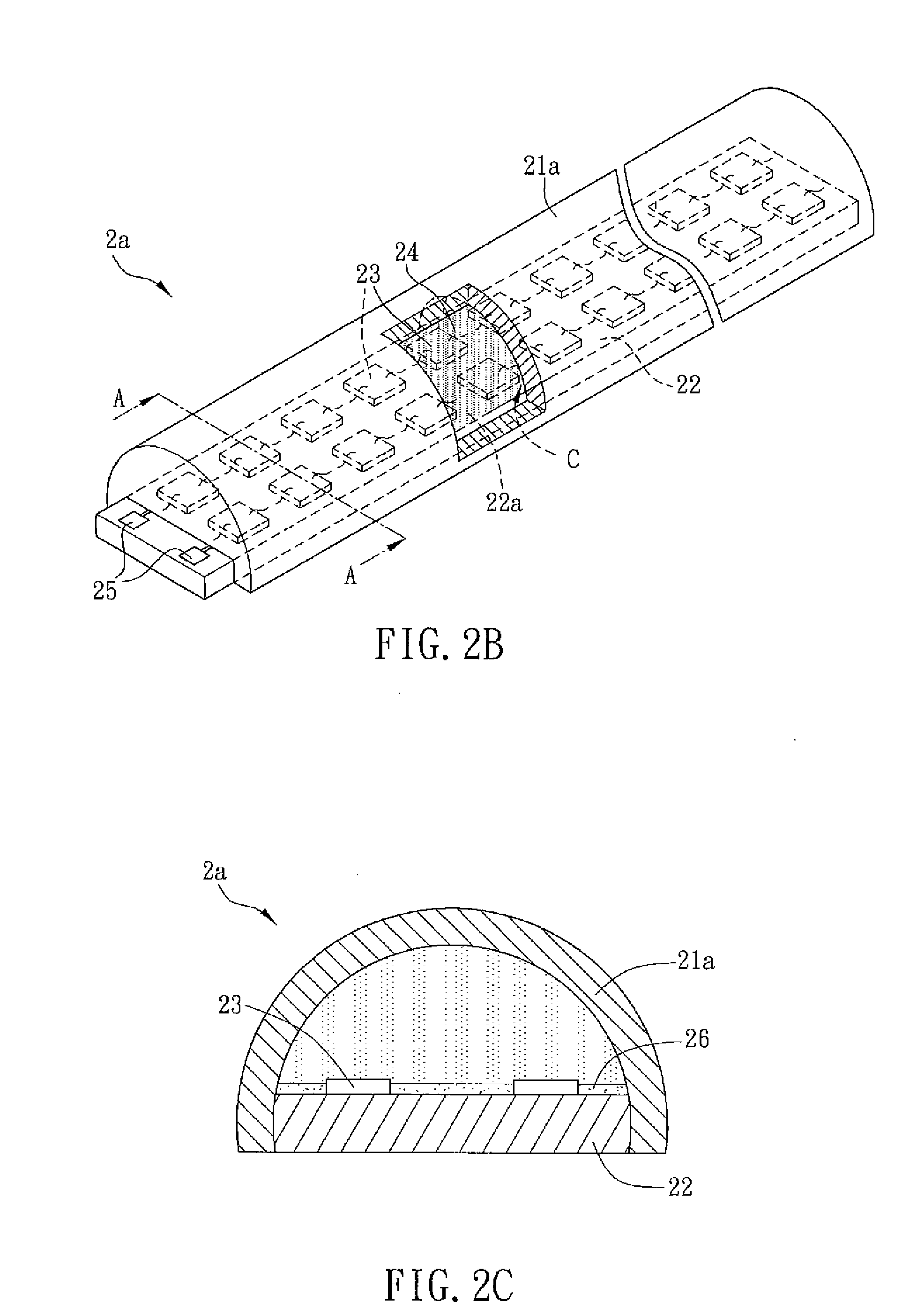
[0040]FIGS. 2A to 2C are schematic views of a light emitting unit according to the embodiment. As shown in FIG. 2A, the light emitting unit 2 includes a housing 21, a substrate 22, a plurality of LED dies 23, and a gel or a fluid 24. In the embodiment, the housing 21 and the substrate 22 form a chamber C for example.

[0041]In the embodiment, the housing 21 is an arc-shape housing for example, and the housing 21 may also be a hemispheric housing. The housing 21 may include a transparent part and a non-transparent part, i.e. the housing 21 may be partially transparent (thus the housing 21 can be called a transparent housing) and partially non-transparent. As a matter of course, the housing 21 may also be entirely transparent. The material of the transparent part is, for example, at least one of polymer, glass, and quartz. The material of the non-transparent part is, for example, at least one of polymer, ceramics, and metal. It is noted that for easily identifying the element, an arc-sh...

second embodiment

[0055]FIGS. 3A and 3B are schematic views of a light emitting unit according to the second embodiment of the present invention, in which FIG. 3B is a cross-sectional view of FIG. 3A along a line C-C. With reference to FIGS. 3A and 3B, the difference between the light emitting unit 3 of the second embodiment and the light emitting 2 of the first embodiment is that the reflecting layer 36 is disposed on the outer surface of the housing 31, and the light emitting unit 3 further includes a wavelength converting material 37 that can be disposed on the partial outer surface and / or the partial inner surface of at least a part of the housing 31, and / or doped in the housing 31.

[0056]The reflecting layer 36 also includes an opening 361 corresponding to a light emitting surface of the LED dies 33. In the embodiment, the wavelength converting material 37 is disposed corresponding to the outer surface of the housing 31 and located at the opening 361 of the reflecting layer 36. The wavelength con...

third embodiment

[0061]FIGS. 4A and 43 are schematic views of a light emitting unit according to the third embodiment of the present invention, in which FIG. 4B is a cross-sectional view of FIG. 4A along a line D-D. With reference to FIGS. 4A and 4B, the light emitting unit 4 according to the embodiment includes a housing 41, a substrate 42, and a plurality of LED dies 43.

[0062]The housing 41 is a metal housing or an alloy housing for example, so the housing 41 has the advantages of high reflectivity, fine heat dissipation effect and can be easily manufactured and formed. The inner surface of the housing 41 is a reflecting surface 411 for example, and the housing 41 and the substrate 42 form a chamber C; the shape of the housing 41 is not limited. The housing 41 has a plurality of concave parts 412 and the reflecting surface 411 is located on the surface of the concave part 412; the concave parts 412 are corresponding to the LED dies 43 for example. As a matter of course, the housing may have only a...


PUM

PropertyMeasurementUnit
reflectivityaaaaaaaaaa
transparentaaaaaaaaaa
wavelengthaaaaaaaaaa

Abstract

A light emitting unit has a chamber. The light emitting unit includes at least one substrate, a plurality of light emitting diode (LED) dies and a gel or a fluid. The LED dies are disposed on the substrate and in the chamber. At least two LED dies are electrically connected to each other in series or in parallel. The gel or the fluid is filled in the chamber.

Description

CROSS REFERENCE TO RELATED APPLICATIONS[0001]This Non-provisional application claims priority under 35 U.S.C. §119(a) on Patent Application No(s). 096145786, 096145787 and 096145788 filed in Taiwan, Republic of China on Nov. 30, 2007, and Patent Application No(s). 097131771 filed in Taiwan, Republic of China on Aug. 20, 2008, the entire contents of which are hereby incorporated by reference.BACKGROUND OF THE INVENTION[0002]1. Field of Invention[0003]The present invention relates to a light emitting unit and, in particular, to a light emitting unit having a chamber.[0004]2. Related Art[0005]Because the light emitting diode (LED) has the advantages of high light intensity and energy saving, as the LED technology is getting matured, it can be applied to more fields such as the light source and the backlight source.[0006]FIG. 1 is a schematic view of a conventional light emitting unit 1. With reference to FIG. 1, the conventional light emitting unit 1 includes a substrate 11, a pluralit...

Claims


Application Information

Patent Timeline
Patent Type & Authority Applications(United States)
IPC IPC(8): H01L33/00H01L33/56
CPCF21V31/04H01L33/56F21V17/04H01L2224/48091H01L2224/8592H01L2224/45144H01L2224/48137H01L2924/1461F21Y2105/10F21K9/64F21Y2103/10F21Y2115/10H01L2924/181F21Y2107/90F21K9/68F21V3/062F21V3/061H01L2924/00014H01L2924/00H01L2924/00012
Inventor SAH, WEN-JYH
Owner GIGNO TECH CO LTD
Why Eureka
Try Eureka