Sensor interface devices and amplifiers

a technology of an interface device and an amplifier, which is applied in the direction of dielectric amplifiers, amplifier types, amplifiers, etc., can solve the problems of chopper offset errors, input signal bandwidth limitations, and the frequency range of flicker noise is posted a limit on lowering the chopper frequency, so as to reduce the dc-offset and flicker noise

Inactive Publication Date: 2009-06-04
THE CHINESE UNIVERSITY OF HONG KONG
View PDF8 Cites 16 Cited by
  • Summary
  • Abstract
  • Description
  • Claims
  • Application Information

AI Technical Summary

Benefits of technology

[0009]Disclosed is a sensor interface device capable of reducing DC-offset and flicker noise without any limitation to an input bandwidth.

Problems solved by technology

A problem with the conventional chopper technique is that the choppers themselves generate offset errors that are indistinguishable from the desired signal.
However, the frequency range of the flicker noise posts a limit on lowering the chopper frequency.
A drawback of the nested chopper technique is that, since the outer choppers operate at a very low frequency, the input signal bandwidth is limited.

Method used


Image

  • Sensor interface devices and amplifiers
  • Sensor interface devices and amplifiers
  • Sensor interface devices and amplifiers

Examples


Embodiment Construction

[0024]The present invention will be described with reference to the accompanying drawings, but these drawings are presented only for the illustrative purpose and in no respect, are intended to limit the present invention anymore.

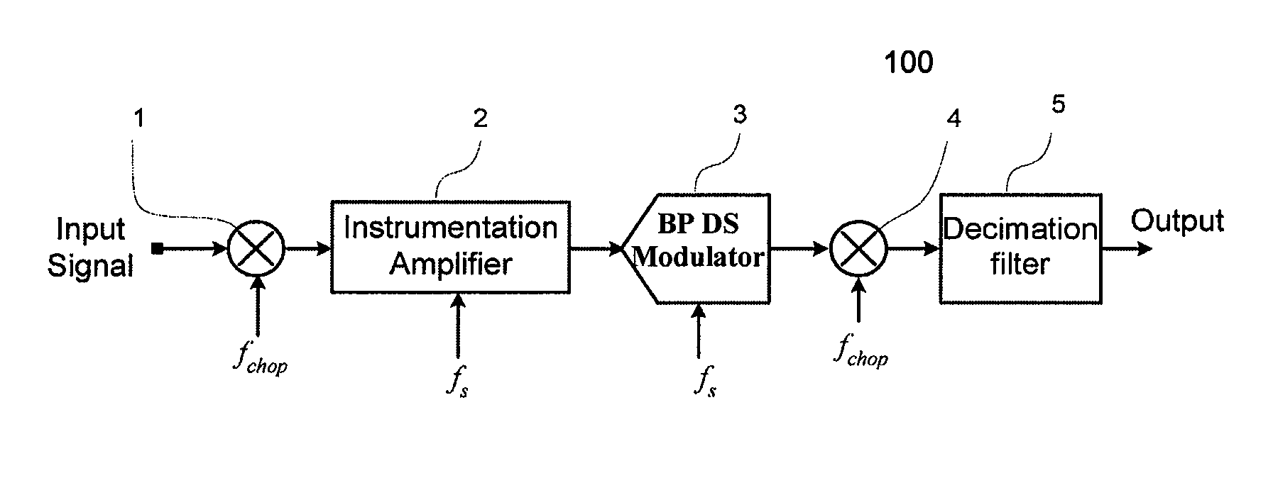
[0025]FIG. 1 is a block diagram of a sensor interface device 100 according to one embodiment of the invention, comprising a first chopper 1, an instrumentation amplifier (IA) 2, a Bandpass (BP) Delta-Sigma A / D converter 3, a second chopper 4 and a decimation filter 5.

[0026]The sensor interface device accepts a voltage-mode input signal. Specifically, as showing in FIG. 1, the first chopper 1 which operates at a frequency denoted as fchop receives an input signal to shift the received signal from the baseband to fchop. Herein, the first chopper 1 is an analog chopper and fchop must be greater than the corner frequency of the flicker noise in the system.

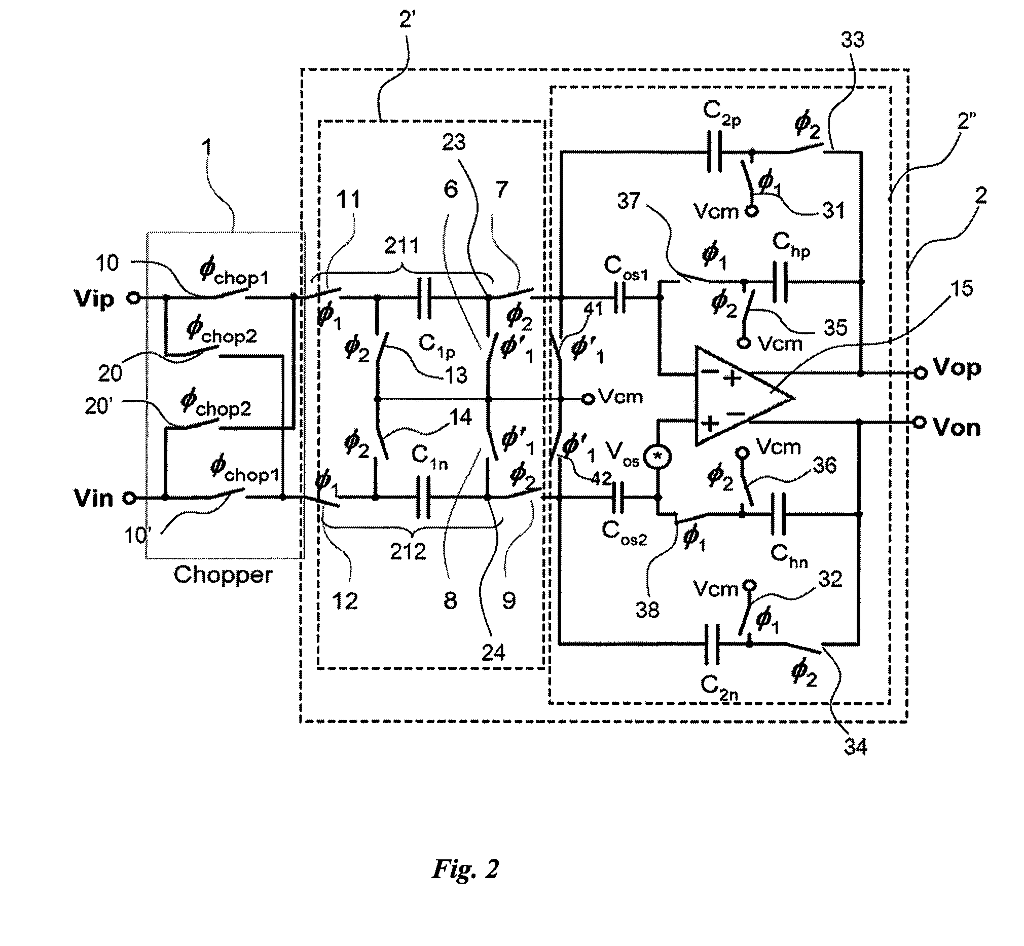
[0027]The IA 2 receives the output from the chopper 1 and amplifies the received signal. The gain of amplifi...


PUM


Abstract

Disclosed are a sensor interface device and an amplifier used in a sensor system. The sensor interface device in one implementation has a first chopper configured to shift input signals of the sensor system from a baseband frequency to a first frequency, an instrumentation amplifier configured to amplify the shifted signals, a bandpass Delta-Sigma modulator configured to digitize the amplified signals, and a second chopper configured to shift the digitized signals from the a first frequency back to the baseband frequency. The instrumentation amplifier removes the DC offset generated from the first chopper and therefore all sources of DC offset are eliminated in this interface device without bandwidth limitation.

Description

CROSS-REFERENCES TO RELATED APPLICATIONS[0001]This application claims the benefit of U.S. Provisional Patent Application Ser. No. 60 / 991,753, filed on Dec. 2, 2007, entitled “Amplifier and Analog-to-digital Converter Circuits Comprising Means for Reducing DC-offset and Flicker Noise”, which is herein incorporated by reference in its entirety.TECHNICAL FIELD OF THE INVENTION[0002]This invention generally relates to a sensor interface device and an amplifier. In particular, the invention relates to a sensor interface device for reducing DC-offset and flicker noise.BACKGROUND OF THE INVENTION[0003]Sensor systems are widely used in the fields of industrial and medical electronics, wherein a sensor interface device is essential to establish a link between a sensor of a sensor system and the rest components of the same.[0004]The sensor systems, to which the invention relates, have two common characteristics. Firstly, the output signal of a sensor in the sensor systems is a voltage quantit...

Claims


Application Information

Patent Timeline
Patent Type & Authority Applications(United States)
IPC IPC(8): H03M3/00H03F21/00
CPCH03M3/458H03M3/34
Inventor PUN, KONG PANGCHOY, CHIU SING OLIVER
Owner THE CHINESE UNIVERSITY OF HONG KONG
Why Eureka
Try Eureka