Thin-film transistor, electro-optical device, and electronic apparatus

a technology of electrooptical devices and transistors, applied in the direction of solid-state devices, semiconductor devices, thermoelectric devices, etc., can solve the problems of inability to produce thin-film transistors, and inability to meet the requirements of high-speed data transmission, etc., to achieve high-reliability

Active Publication Date: 2009-06-11
E INK CORPORATION
View PDF4 Cites 12 Cited by
  • Summary
  • Abstract
  • Description
  • Claims
  • Application Information

AI Technical Summary

Benefits of technology

[0043]Thus, the electronic apparatus has highly reliable.

Problems solved by technology

However, it has been significantly difficult to produce thin-film transistors that allow a large current to flow in an ON state.
Although thin-film transistors that allow a larger current to flow in an ON state have been able to be produced, a problem of current flow in an OFF state has arisen.
A problem in which the OFF-state current flows is more noticeable when a thiophene-based material is used as the organic semiconductor material.

Method used


Image

  • Thin-film transistor, electro-optical device, and electronic apparatus
  • Thin-film transistor, electro-optical device, and electronic apparatus
  • Thin-film transistor, electro-optical device, and electronic apparatus

Examples


first embodiment

[0055]A first embodiment of the invention will be described below.

(1) Thin-Film Transistor

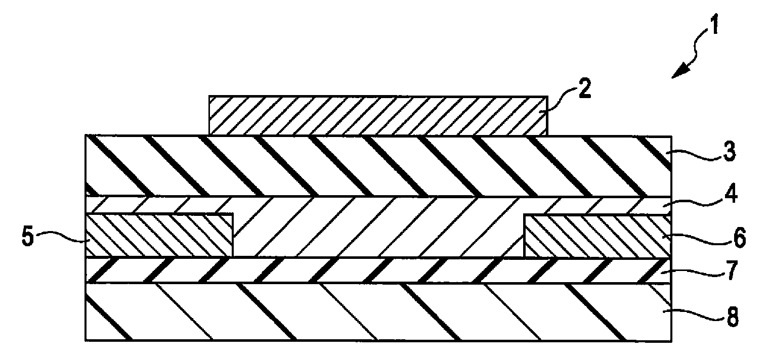
[0056]FIG. 1 shows a thin-film transistor according to the first embodiment of the invention and is a schematic longitudinal sectional view of a thin-film transistor 1. In the following description, the upper side and the lower side in FIG. 1 is defined as the upper side and the lower side of the thin-film transistor 1.

[0057]The thin-film transistor 1 according to this embodiment shown in FIG. 1 includes a gate electrode 2, a first insulating layer 3, an organic semiconductor layer 4, a source electrode 5, a drain electrode 6, and a second insulating layer 7. The second insulating layer 7, the source electrode 5 and the drain electrode 6, the organic semiconductor layer 4, the first insulating layer 3, and the gate electrode 2 are formed in that order on a substrate 8. That is, the thin-film transistor 1 according to this embodiment is a top-gate bottom-contact organic thin-film transistor.

[005...

second embodiment

[0142]While a thin-film transistor 1 and a method for producing the same according to a second embodiment will be described below, differences between the first embodiment and the second embodiment will be mainly described. Descriptions of equivalent items are not redundantly repeated.

(1) Thin-Film Transistor

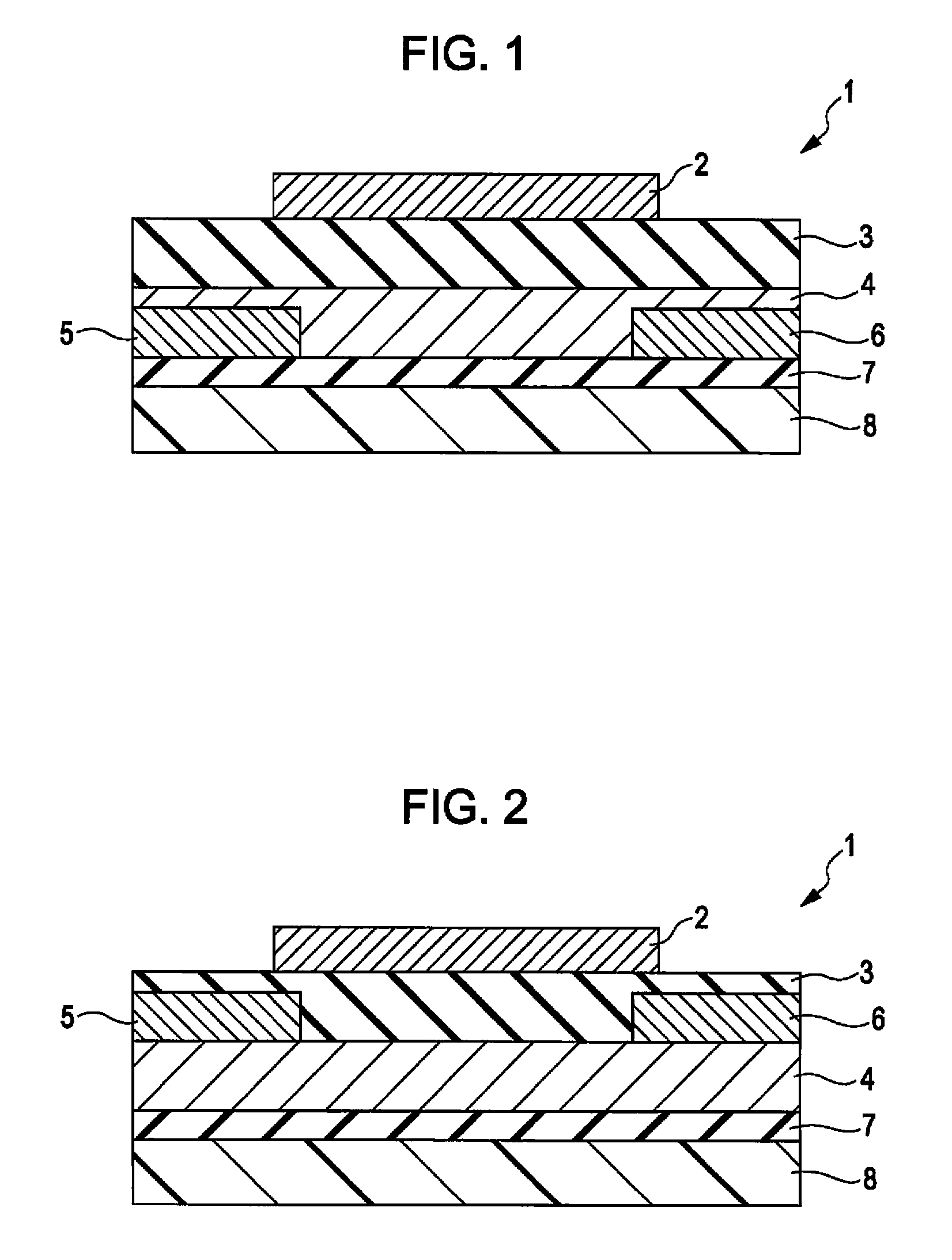
[0143]FIG. 2 shows a thin-film transistor according to the second embodiment of the invention and is a schematic longitudinal sectional view of a thin-film transistor 1. In the following description, the upper side and the lower side in FIG. 2 is defined as the upper side and the lower side of the thin-film transistor 1.

[0144]The thin-film transistor 1 according to this embodiment is the same as in the first embodiment, except that the source electrode 5 and the drain electrode 6 are in contact with upper surfaces of portions of the organic semiconductor layer 4 overlapping the source electrode 5 and the drain electrode 6 in plan.

[0145]In other words, the thin-film transistor 1 ...

third embodiment

[0155]While a thin-film transistor 1 and a method for producing the same according to a third embodiment will be described below, differences between the first embodiment and the third embodiment will be mainly described. Descriptions of equivalent items are not redundantly repeated.

(1) Thin-Film Transistor

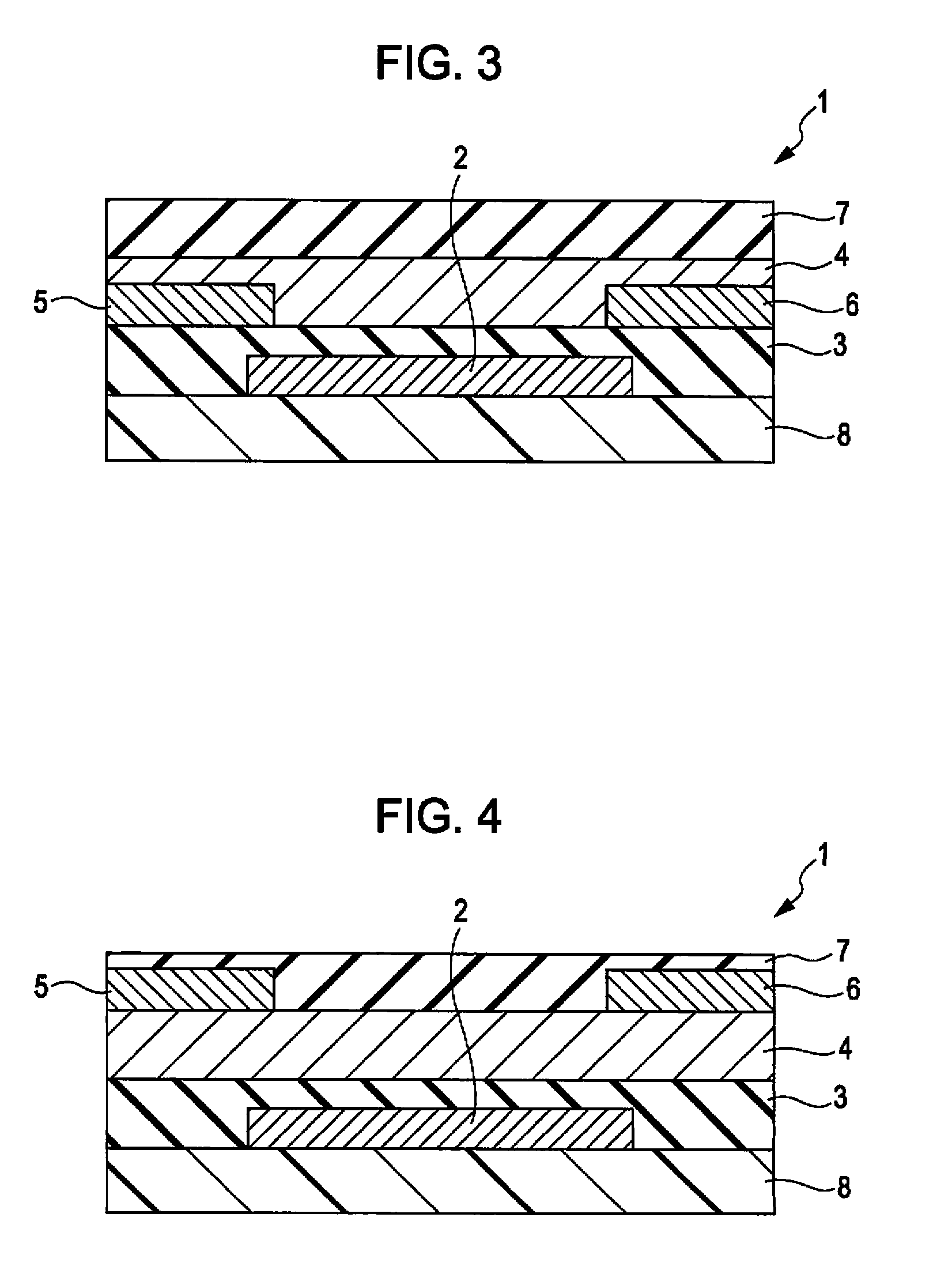
[0156]FIG. 3 shows a thin-film transistor according to the third embodiment of the invention and is a schematic longitudinal sectional view of a thin-film transistor 1. In the following description, the upper side and the lower side in FIG. 3 is defined as the upper side and the lower side of the thin-film transistor 1.

[0157]The thin-film transistor 1 according to this embodiment is the same as in the first embodiment, except that the gate electrode 2 is located closer to the substrate 8 than the source electrode 5 and the drain electrode 6 and that the source electrode 5 and the drain electrode 6 are in contact with lower surfaces of portions of the organic semiconductor layer 4 ...


PUM

PropertyMeasurementUnit
thicknessaaaaaaaaaa
thicknessaaaaaaaaaa
thicknessaaaaaaaaaa

Abstract

A thin-film transistor includes a source electrode, a drain electrode arranged apart from the source electrode, an organic semiconductor layer arranged between the source electrode and the drain electrode so as to establish connection of the source electrode and the drain electrode, a first insulating layer arranged on one surface side of the organic semiconductor layer, a gate electrode arranged on a side of the first insulating layer opposite that on which the organic semiconductor layer lie, and a second insulating layer arranged on a side of the organic semiconductor layer opposite that on which the first insulating layer lie. The organic semiconductor layer contains an organic semiconductor material having p-type semiconducting properties. The second insulating layer contains one or more compounds of the following formula (1), so that electrons are fed from the second insulating layer into the organic semiconductor layer:
wherein R1 and R2 independently represent a substituted or unsubstituted alkylene group; X1, X2, X3 and X4 each represent a hydrogen atom or an electron-donating group; and n represents 100 to 100,000, wherein at least one of X1, X2, X3 and X4 represents an electron-donating group.

Description

BACKGROUND[0001]1. Technical Field[0002]The present invention relates to thin-film transistors, electro-optical devices, and electronic apparatuses.[0003]2. Related Art[0004]In recent years, organic thin-film field-effect transistors composed of organic semiconductor materials have been receiving attention as devices that would substitute for thin-film field-effect transistors composed of inorganic materials such as silicon.[0005]The reason for this is as follows: for example, (I) since organic thin-film field-effect transistors can be produced at lower temperatures than those of transistors composed of inorganic semiconductor materials, plastic substrates and films can be used as substrates. This makes it possible to produce flexible, lightweight, and durable thin-film transistors; (II) thin-film transistors can be produced in a short period of time by simple methods, such as application methods and printing, including supplying solutions containing organic materials, thereby achie...

Claims


Application Information

Patent Timeline
Patent Type & Authority Applications(United States)
IPC IPC(8): H01L51/05
CPCH01L51/0035H01L51/0558H01L51/0512Y02E10/549H10K85/111H10K10/462H10K10/484H10K77/10
Inventor AOKI, TAKASHI
Owner E INK CORPORATION
Why Eureka
Try Eureka