
Backside illuminated image sensor

a backside and image sensor technology, applied in the field of image sensors, can solve problems such as image loss

Active Publication Date: 2009-06-11
INTELLECTUAL VENTURES II
View PDF10 Cites 95 Cited by
  • Summary
  • Abstract
  • Description
  • Claims
  • Application Information

AI Technical Summary

Problems solved by technology

Accordingly, an amount of light that one light receiving element can collect is reduced and noise is increased, causing various problems such as image loss.

Method used


Image

  • Backside illuminated image sensor
  • Backside illuminated image sensor
  • Backside illuminated image sensor

Examples


first embodiment

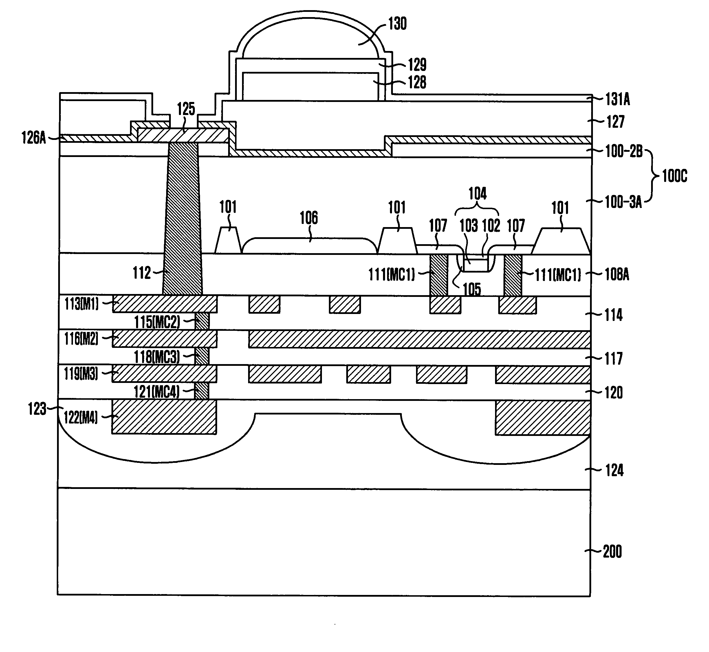
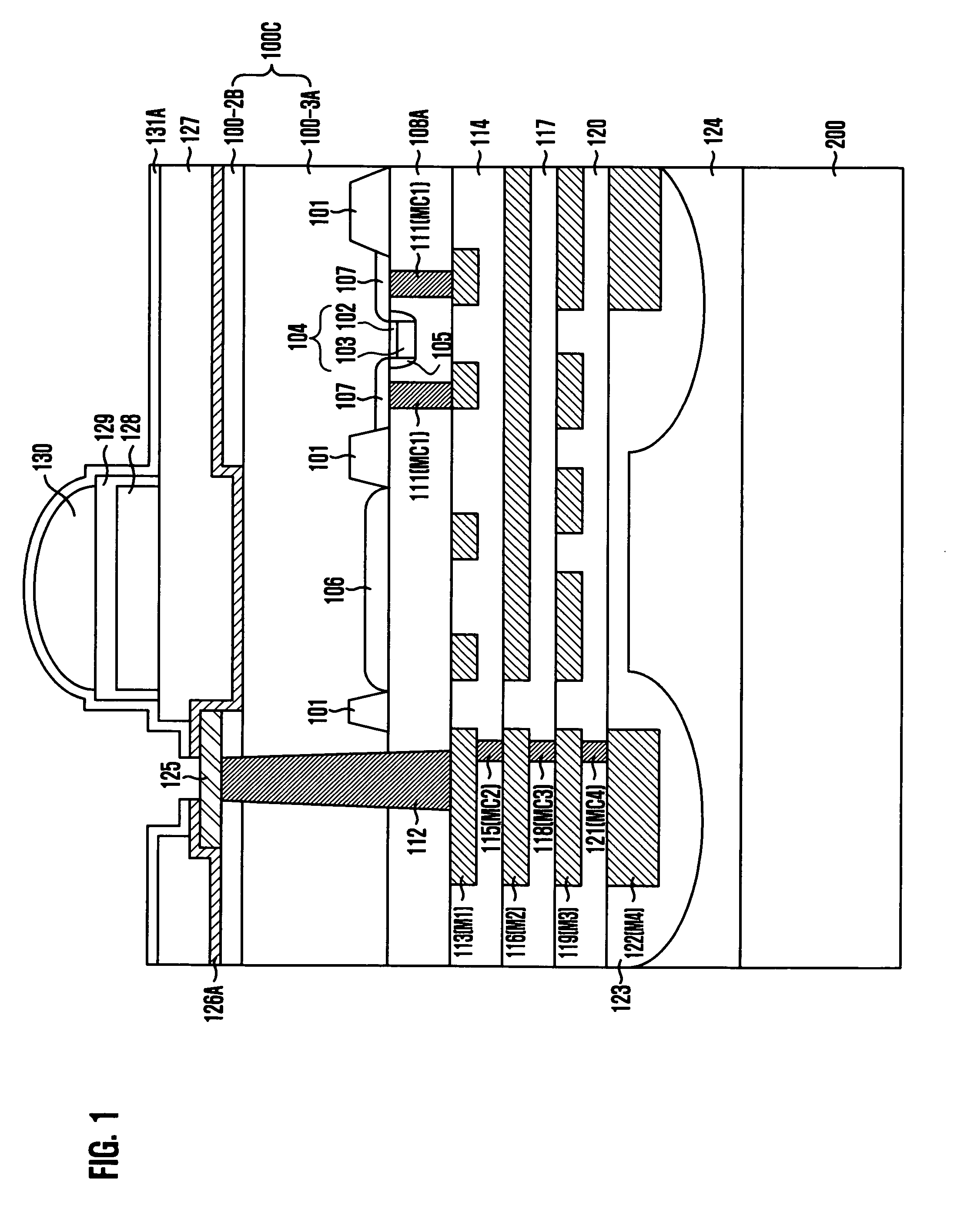
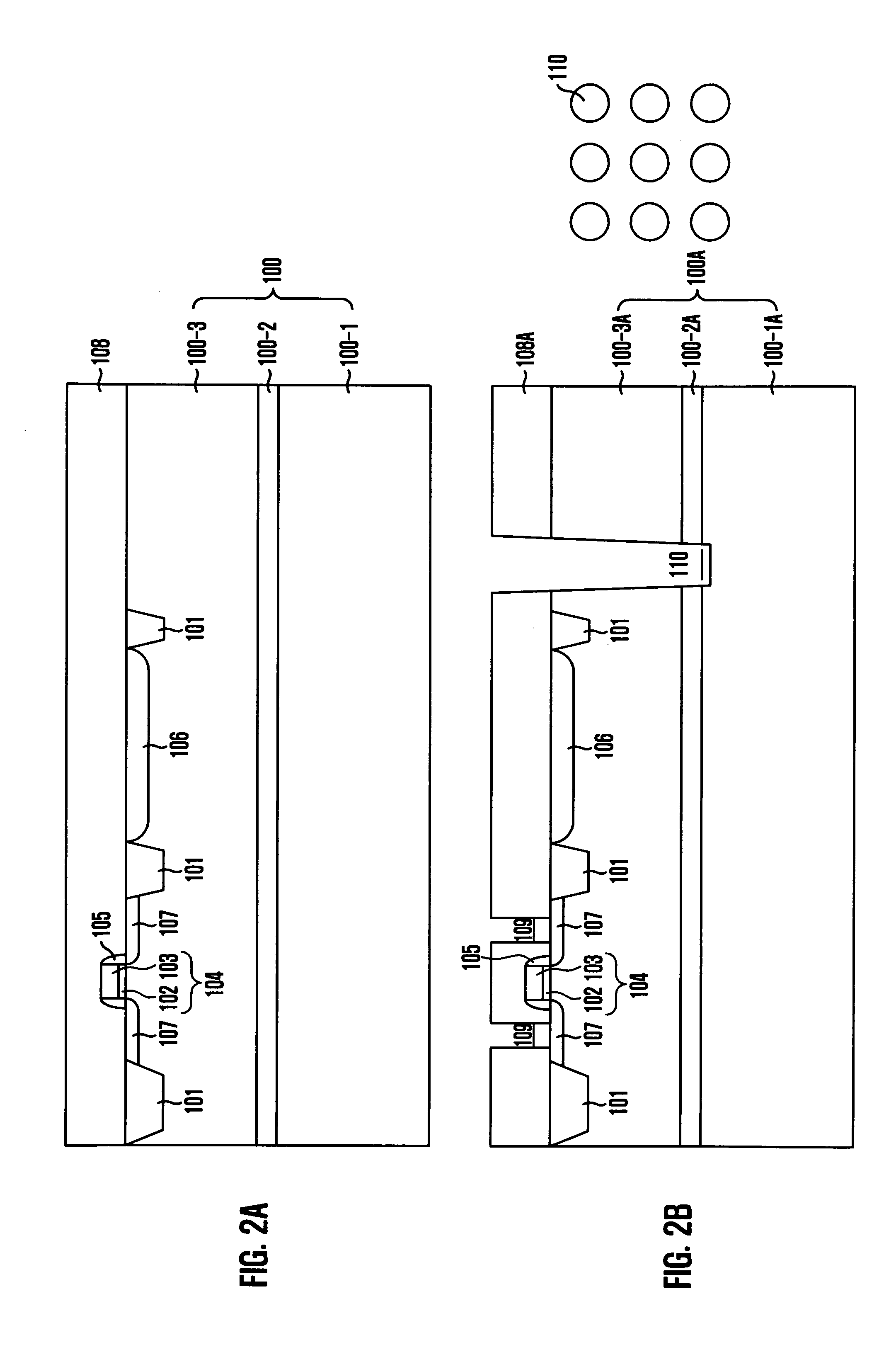
[0012]FIG. 1 illustrates a cross-sectional view of a backside illuminated image sensor in accordance with the present invention. Only a photo diode and a gate electrode of a driving transistor in a unit pixel of a CMOS image sensor are illustrated in FIG. 1 for convenience.

[0013]Referring to FIG. 1, the backside illuminated image sensor in accordance with the first embodiment of the present invention has a structure in which a device wafer and a handle wafer are attached together. The device wafer is a wafer where a light receiving element such as a photodiode is formed, and the handle wafer is a wafer where peripheral circuits such as a digital block and an analog-to-digital converter are formed. In the following description, the device wafer and the handle wafer will be referred to as a first substrate and a second substrate, respectively.

[0014]The backside illuminated image sensor in accordance with the first embodiment of the present invention includes a light receiving element,...

second embodiment

[0066]FIG. 3 illustrates a cross-sectional view of a backside illuminated image sensor in accordance with the present invention. Only a photo diode and a gate electrode including a driving transistor in a unit pixel of a CMOS image sensor are illustrated for convenience.

[0067]Referring to FIG. 3, the backside illuminated image sensor in accordance with the second embodiment of the present invention includes a light receiving element, for example, a photodiode 306, which is formed in a first substrate 300D, a remaining interlayer insulation pattern 308B formed over the first substrate 300D including the photodiode 306, an align key pattern 312A spaced apart from the photodiode 306 and passing through the remaining interlayer insulation pattern 308B and the first substrate 300D, first to fourth interconnection layers 313, 316, 319 and 322 formed over the remaining interlayer insulation pattern 308B in a multi-layered structure, where the backside of the first interconnection layer 313...


PUM


Abstract

A backside illuminated image sensor includes a light receiving element disposed in a first substrate, an interlayer insulation layer disposed on the first substrate having the light receiving element, an align key spaced apart from the light receiving element and passing through the interlayer insulation layer and the first substrate, a plurality of interconnection layers disposed on the interlayer insulation layer in a multi-layered structure, wherein the backside of the lowermost interconnection layer is connected to the align key, a passivation layer covering the interconnection layers, a pad locally disposed on the backside of the first substrate and connected to the backside of the align key, a light anti-scattering layer disposed on the backside of the substrate having the pad, and a color filter and a microlens disposed on the light anti-scattering layer to face the light receiving element.

Description

CROSS-REFERENCE TO RELATED APPLICATIONS[0001]The present invention claims priority of Korean patent application numbers 10-2007-0125506, 10-2007-00125507, and 10-2008-0036203, filed on Dec. 5, 2007, Dec. 5, 2007, and Apr. 18, 2008, respectively, which are incorporated by reference in their entirety.BACKGROUND OF THE INVENTION[0002]The present invention relates to an image sensor, and more particularly, to a backside illuminated image sensor.[0003]In a complementary metal oxide semiconductor (CMOS) image sensor, a light receiving element, a digital control block, and a peripheral circuit such as an analog-to-digital converter are arranged at a finite area within a chip. Thus, an area ratio of a pixel array per a chip area is limited to about 40%. Furthermore, a pixel size is greatly reduced for implementation of high quality images. Accordingly, an amount of light that one light receiving element can collect is reduced and noise is increased, causing various problems such as image lo...

Claims


Application Information

Patent Timeline
IPC IPC(8): H01L31/12
CPCH01L27/14632H01L27/1464H01L27/14687H01L27/14636H01L21/76898H01L23/481H01L2924/0002H01L2924/00
Inventor PYO, SUNG-GYU
Owner INTELLECTUAL VENTURES II
Features
  • Generate Ideas
  • Intellectual Property
  • Life Sciences
  • Materials
  • Tech Scout
  • Unparalleled Data Quality
  • Higher Quality Content
  • 60% Fewer Hallucinations
Learn More