

Nanostructure-Film LCD Devices
a technology of nanostructure films and display devices, applied in the field of nanostructure films, can solve the problems of insufficient solution, inferior flexibility, and the indium component of ito is rapidly becoming a scarce commodity, and achieves extraordinary strength and electrical conductivity, efficient heat conduction, and exceptional material properties.
- Summary
- Abstract
- Description
- Claims
- Application Information
AI Technical Summary
Benefits of technology
Problems solved by technology
Method used
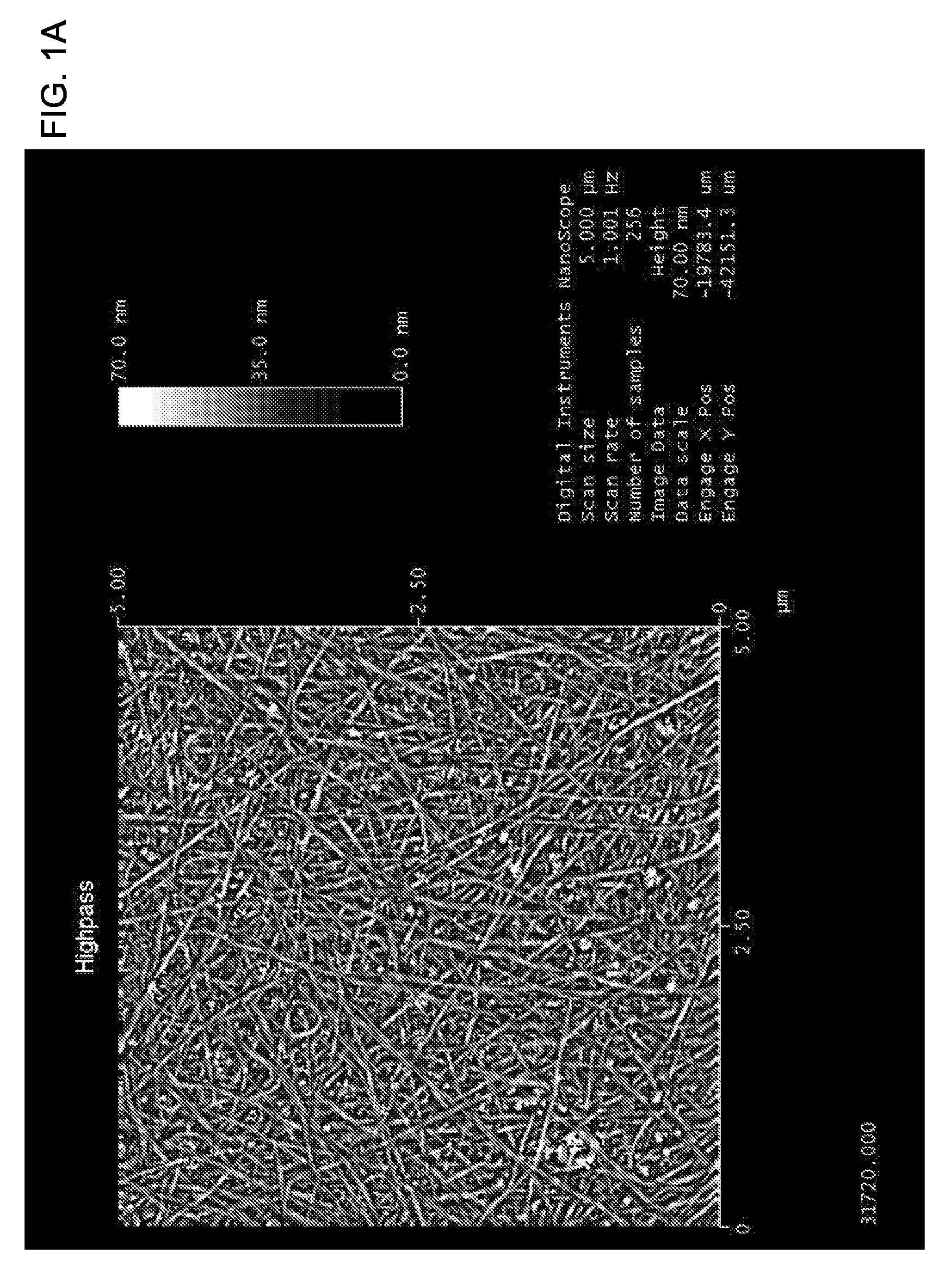
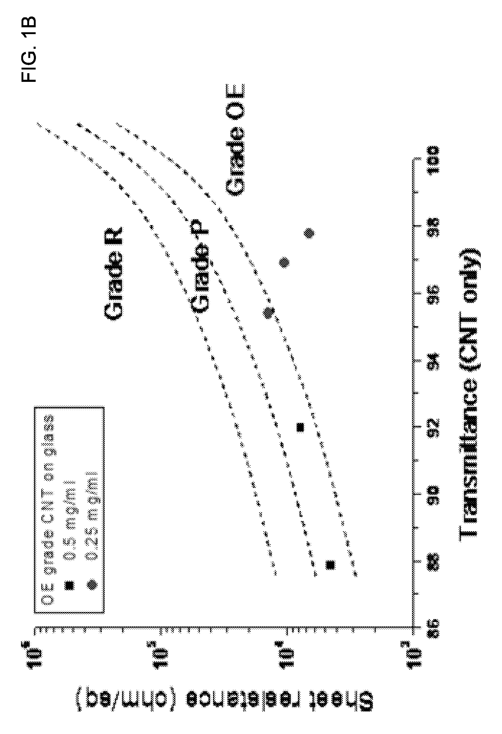
Image

Examples
Embodiment Construction
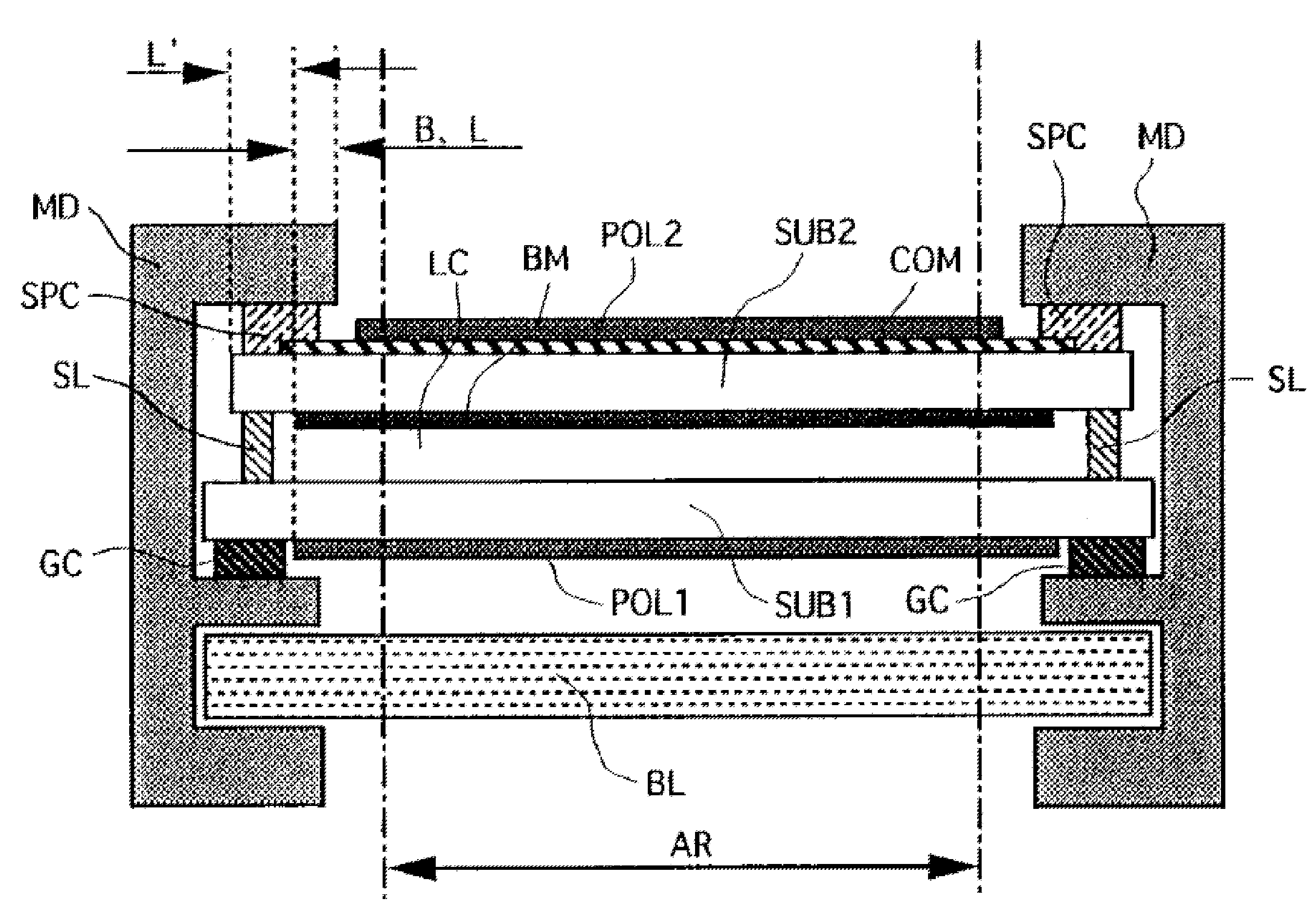
[0032]In one embodiment, an electrically conductive and optically transparent nanostructure film, for example as described above, may be employed in an in-plane switching (IPS) LCD device to serve a shielding function against static electricity. The IPS LCD device may include a switching element, a pixel electrode and a counter electrode formed in a unit pixel over a first substrate of two substrates which are so disposed as to be opposed to each with a liquid crystal layer provided there between and at least one of the two substrates is transparent, and the light that passes through the liquid crystal layer is modulated with an electric field generated between the pixel electrode and the counter electrode substantially in parallel with the first substrate; wherein a black matrix having a resistivity of not smaller than 106 ohm-cm is formed between the first substrate and the second substrate, and an electrically conductive and optically transparent nanostructure film is formed over...
PUM
| Property | Measurement | Unit |
|---|---|---|
| semi-transparent | aaaaa | aaaaa |
| sheet resistance | aaaaa | aaaaa |
| sheet resistance | aaaaa | aaaaa |
Abstract
Description
Claims
Application Information