Optical element for x-ray

a technology of optical elements and x-rays, applied in the field of optical elements for x-ray, can solve the problems of reducing lowering the optical aberration performance, and reducing the film stress, so as to achieve high optical performance and suppress the surface shape error

Inactive Publication Date: 2009-06-11
CANON KK
View PDF3 Cites 5 Cited by
  • Summary
  • Abstract
  • Description
  • Claims
  • Application Information

AI Technical Summary

Benefits of technology

[0020]For optimizing a periodic structure of the second multilayer film, a necessary pair number is reduced by increasing unit period thickness to suppress a total film thickness. In addition, the unit period thickness is made a two or more integral multiple of 7 nm, so that it is possible to carry out film thickness measurement with a spectrophotometer and film thickness control with accuracy during film formation. As a result, it is possible to provide an optical element for X-ray in which film thickness non-uniformity is suppressed to suppress a surface shape error and a high optical performance is achieved.

Problems solved by technology

On the other hand, with respect to practical application of the multilayer film reflecting mirror, it remains many problems such as prevention of lowering in refractive index, light resistance, film thickness distribution control for obtaining a desired film thickness distribution in a plane of the optical element, suppression of film stress causing a deformation of an optical element surface, and the like.
Particularly, when a manufacturing error in film thickness distribution occurs, a surface shape of an optical element surface-polished precisely is changed depending on optical design.
This is an important problem since an optical aberration performance of the exposure device is considerably lowered.
Further, the film stress also changes the surface shape of the optical element to cause the lowering in optical aberration performance, so that the suppression of the film stress is also an important problem.
However, the above-described conventional methods for preventing the deformation of the substrate due to the film stress of the multilayer film in the multilayer film reflecting mirror have accompanied with the following problems.
However, in these methods, it was difficult to carry out film thickness measurement with accuracy meeting a requirement for an exposure device particularly in an X-ray range.
For this reason, even when the stress buffering layer formed on the substrate causes film thickness non-uniformity depending on its position, film thickness control cannot be carried out at a level less than an accuracy level of the film thickness measurement.
That is, in the case where the stress buffering layer consisting of the single layer is used in the optical element such as the exposure device or the like, the film thickness cannot be measured even when the film thickness non-uniformity occurs in the stress buffering layer.
When the film thickness non-uniformity is present in the stress buffering layer, a surface shape of the reflection layer formed on the stress buffering layer is also changed, thus resulting in a surface shape error of the optical element.
For that reason, the total film thickness is large even when each of the layers causes slight film thickness non-uniformity.
As a result, the film thickness non-uniformity of the stress buffering layer is increased to result in the surface shape error of the optical element, thus leading to deterioration of an exposure performance of the exposure device.
For that reason, sufficient removal of the film stress cannot be achieved, so that it remains the film stress.
After all, the pair number of the stress buffering layer is required to be increased to such an extent that the stress buffering layer can sufficiently remove the film stress, so that the constitution of JP-A 2002-525698 is accompanied with the same problem as in JP-A 2002-504715 which is a potential caused of the surface shape error of the optical element.

Method used


Image

  • Optical element for x-ray
  • Optical element for x-ray
  • Optical element for x-ray

Examples


embodiment 1

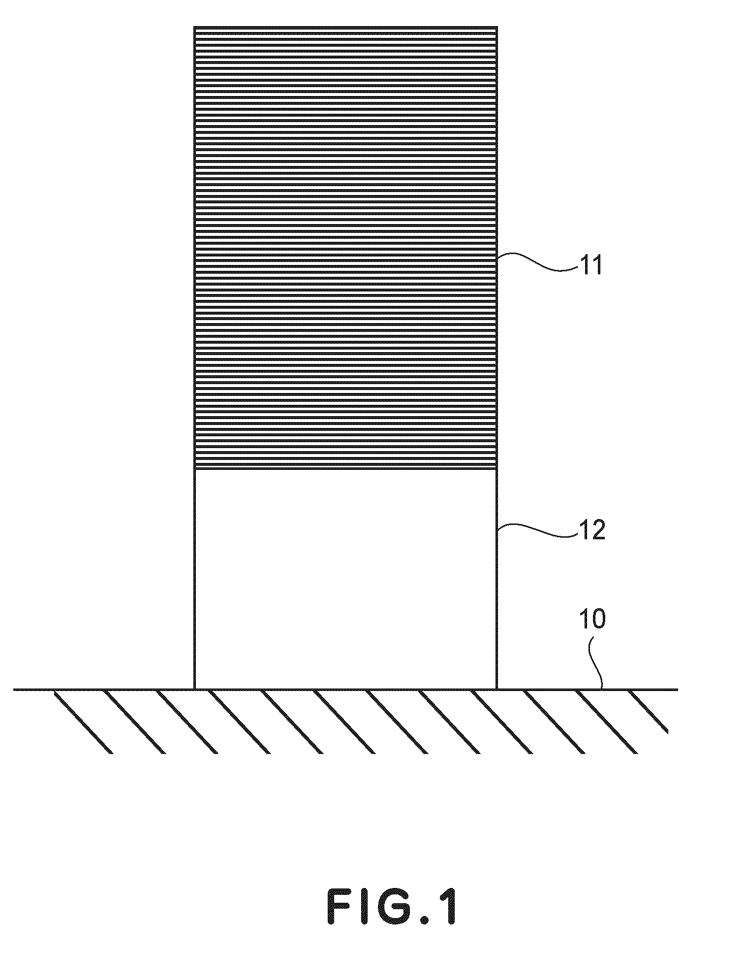
[0043]FIG. 1 shows an optical element for X-ray functioning as a reflecting mirror in an X-ray optical system in this embodiment. A first multilayer film 11 having a high reflection characteristic in a soft X-ray wavelength range is constituted by alternating layers of Mo / Si. A film having the same film structure as the first multilayer film 11 is formed on a test piece such as an Si wafer or the like and a surface shape of the test piece is measured before and after the film formation by an interferometer and then film stress is calculated from an amount of change in surface shape of the test piece and Young's modulus. As a result, the film stress of this multilayer film alone was −98.3 N / m2.

[0044]A second multilayer film 12 occupying a space between the first multilayer film 11 and a substrate 10 has a periodic structure which is formed by alternately laminating an Mo layer and an Si layer so that a unit period thickness which is a film thickness of a pair of Mo / Si layers is withi...

embodiment 2

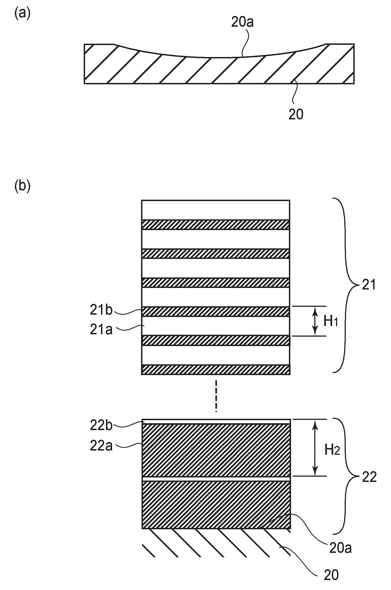
[0050]FIG. 3(a) is a schematic sectional view showing a concave reflecting mirror for X-ray as an optical element for X-ray in this embodiment, wherein a substrate 20 is constituted by a known low thermal expansion optical material (“ZERODUR”) and has a curved surface 20a which has been subjected to optical polishing. On the curved surface 20a, a first multilayer film 21 as an upper multilayer film and a second multilayer film 22 as a lower multilayer film are formed as shown in FIG. 3(b).

[0051]The first multilayer film 21 has a unit period thickness H1 and is constituted by alternating films of an Si layer 21a and an Mo layer 21b. The second multilayer film 22 has a unit period thickness H2 and is constituted by alternating films of an Si layer 22a and an Mo layer 22b.

[0052]The substrate 20 is formed of the material (“ZERODUR”).

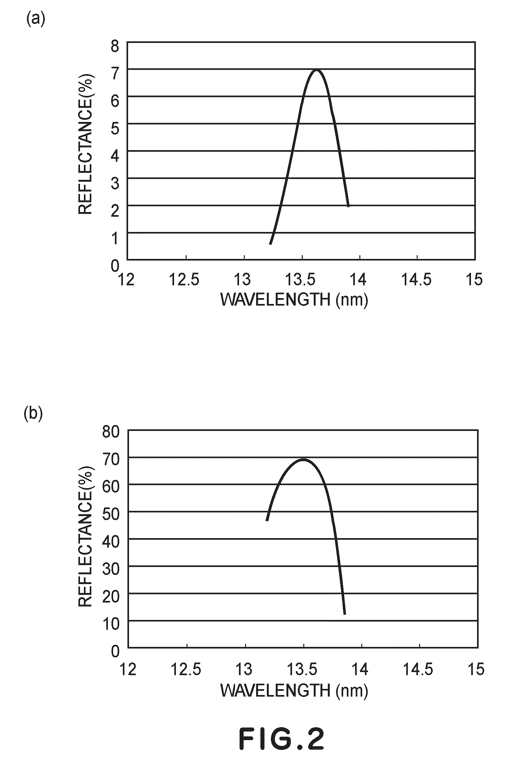
[0053]In order to determine a film forming condition when the first and second multilayer films 21 and 22 are formed, optimization of the film forming cond...


PUM

PropertyMeasurementUnit
thicknessaaaaaaaaaa
thicknessaaaaaaaaaa
thicknessaaaaaaaaaa

Abstract

An optical element for X-ray includes a substrate, a first multilayer film having a reflection property with respect to light in a soft X-ray wavelength range, and a second multilayer film, disposed between the substrate and the first multilayer film, for reducing film stress of the first multilayer film. The second multilayer film has a periodic structure having a unit period film thickness which is 90% or more and less than 110% of a two or more integral multiple of 7 nm.

Description

FIELD OF THE INVENTION AND RELATED ART[0001]The present invention relates to an optical element for X-ray used as a multilayer film reflecting mirror for use in an optical system for an exposure device.[0002]Generally, with respect to light in an X-ray wavelength range of 40 nm or less, a refractive index of a substance is represented by n=1−δ−iβ (δ, β: positive real number), wherein both of δ and β are very smaller than 1 (imaginary part β of the refractive index represents absorption of X-ray). Therefore, the refractive index is substantially close to 1, so that X-ray is little refracted.[0003]For that reason, a lens utilizing refraction of light in a visible light range cannot be used for induction of light in an X-ray wavelength range. Therefore, an optical element utilizing reflection is used for the light induction but the refractive index is also close to 1, so that a reflectance is very low. As a result, almost all part of X-ray passes through or is absorbed by the optical e...

Claims


Application Information

Patent Timeline
Patent Type & Authority Applications(United States)
IPC IPC(8): B32B5/00
CPCB82Y10/00Y10T428/26G21K2201/067G21K1/062
Inventor MIURA, TAKAYUKIANDO, KENJIKANAZAWA, HIDEHIROTERANISHI, KOJIMATSUMOTO, SEIKENNAGATA, KYOKOTATSUMI, SHUMPEIFUKUI, SHINJI
Owner CANON KK
Why Eureka
Try Eureka