Package for semiconductor device and method of manufacturing the same

a semiconductor device and packaging technology, applied in the direction of insulated conductors, power cables, cables, etc., can solve the problems of long processing time, increased cost, and inability to reduce the diameter and pitch of the through hole, so as to achieve high density wiring and reduce resistance value

Active Publication Date: 2009-06-18
SHINKO ELECTRIC IND CO LTD
View PDF13 Cites 3 Cited by
  • Summary
  • Abstract
  • Description
  • Claims
  • Application Information

AI Technical Summary

Benefits of technology

[0007]Exemplary embodiments of the present invention provide a package for a semiconductor device in which a high density wiring can be carried out and a resistance value can be reduced, and a method of manufacturing the package for a semiconductor device

Problems solved by technology

However, the related-art package for a semiconductor device has the following problems.
For this reason, there is a problem in that a long time is required for a processing and a cost is increased.
In the case in which the hole is formed by means of the drill, moreover, a hole diameter and a pitch of the through hole cannot be reduced.
Therefore, there is a problem in that a wiring density cannot be increased.
For this reason, there is a problem in that it is hard to increase a thickness and a resistance value is increased.

Method used


Image

  • Package for semiconductor device and method of manufacturing the same
  • Package for semiconductor device and method of manufacturing the same
  • Package for semiconductor device and method of manufacturing the same

Examples


Embodiment Construction

[0035]The best embodiments according to the invention will be described below in detail with reference to the accompanying drawings.

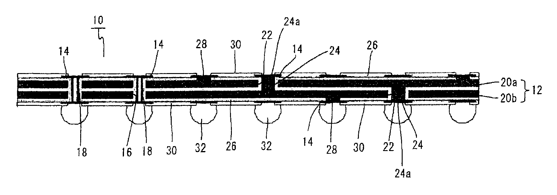
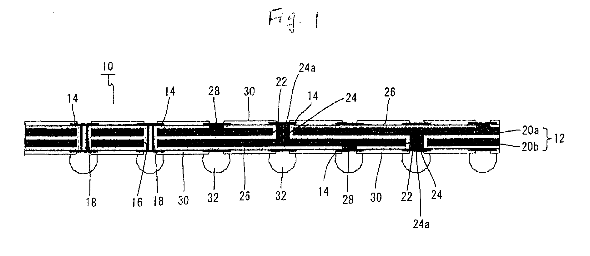
[0036]FIG. 1 is a sectional view showing a package 10 for a semiconductor device according to the embodiment.

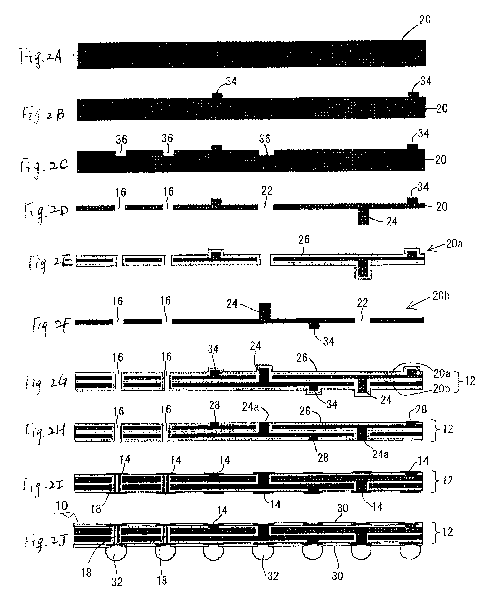
[0037]The package 10 for a semiconductor device has a structure in which wiring patterns 14 are formed on a front surface and a back surface of a core substrate 12 and is connected electrically through a conducting portion 18 formed on a through hole 16 penetrating the core substrate 12.

[0038]The core substrate 12 is formed by integrally providing the first through hole 16 for the conducting portion 18, a second through hole 22 and a projection 24 in each of two metal plates 20a and 20b, forming an insulating layer 26 on surfaces of each of the two metal plates 20a and 20b, and stacking the two metal plates 20a and 20b in such a manner that the projections 24 of the mutual metal plates 20a and 20b enter the second through hole 22 of the metal pla...


PUM

PropertyMeasurementUnit
thicknessaaaaaaaaaa
hole diametersaaaaaaaaaa

Abstract

In a package for a semiconductor device, a core substrate has two metal plates, each of which includes a first through hole, a second through hole, a projection, and an insulating layer formed on its surface. The metal plates are stacked in a manner that the projections of the mutual metal plates enter the second through hole of the metal plate on a partner side, and the first through holes of the metal plates form a through hole penetrating the core substrate. A tip end of each of the projections of the metal plates is exposed to a surface of the metal plate on the partner side to form a first terminal portion, and a second terminal portion is exposed from the insulating layer and formed on a surface of the metal plate on a side where the first terminal portion of the metal plate on the partner side is exposed.

Description

TECHNICAL FIELD[0001]The present disclosure relates to a package for a semiconductor device and a method of manufacturing the package for a semiconductor device.RELATED ART[0002]Referring to a so-called buildup wiring board (a package for a semiconductor device), a through hole is formed on a core substrate (a glass epoxy resin substrate), to both surfaces of which coppers are laminated, by means of a drill, electroless copper plating and electrolytic copper plating are carried out to the core substrate, an etching processing is carried out to form wiring patterns to be electrically connected by a through hole plating coating (a conducting portion) on the both surfaces of the core substrate, and furthermore, a multilayered wiring pattern is formed by a buildup method (Patent Document 1).[0003][Patent Document 1] Japanese Patent Unexamined Publication No. 11-68319[0004]However, the related-art package for a semiconductor device has the following problems.[0005]More specifically, it i...

Claims


Application Information

Patent Timeline
Patent Type & Authority Applications(United States)
IPC IPC(8): H05K1/11H01R43/00
CPCH01L21/4846Y10T29/49117H01L23/49822H05K3/06H05K3/4608H05K3/4641H05K2201/0355H05K2203/0369H05K2203/0733H05K2203/1476H01L2924/0002H01L2924/15311H01L23/142Y10T29/49169Y10T29/49128Y10T29/49126Y10T29/49147Y10T29/49155H01L2924/00H05K3/34H05K3/40
Inventor KOIZUMI, NAOYUKIOI, KIYOSHITATEIWA, AKIHIKO
Owner SHINKO ELECTRIC IND CO LTD
Why Eureka
Try Eureka