
High-power, broad-band, superluminescent diode and method of fabricating the same

a superluminescent diode and wavelength band technology, applied in the field of optical devices with high optical power and a broad wavelength band, can solve the problems of excessively low optical power of the sld according to the paper of ong et al., difficult to provide a required high optical power, and large wavelength bandwidth of the sld, etc., to achieve low optical confinement factor, and high optical confinement factor

Active Publication Date: 2009-06-18
ELECTRONICS & TELECOMM RES INST
View PDF3 Cites 13 Cited by
  • Summary
  • Abstract
  • Description
  • Claims
  • Application Information

AI Technical Summary

Benefits of technology

The present invention provides a superluminescent diode with high optical power and wide optical bandwidth. The diode includes a quantum well structure with a high optical confinement factor region and a low optical confinement factor region. The diode can be fabricated using a selective area growth method, which allows for the formation of the regions with different optical confinement factors. The high optical confinement factor region generates a high-output light, while the low optical confinement factor region reduces saturation of an optical gain in order to amplify light in a broad wavelength band. The output and wavelength bandwidth of the emitted light can be adjusted by adjusting the length of the active layers with different optical confinement factors. The width of a quantum well is smaller in the active layer with the lower optical confinement factor, which prevents saturation of the active layer with the higher optical confinement factor.

Problems solved by technology

However, these methods may increase a wavelength bandwidth of the SLD, but have a limitation in that it is difficult to provide a required high optical power.
For example, the optical power of the SLD according to the paper of Ong et al. is excessively low, e.g., about 1.5 mW.

Method used


Image

  • High-power, broad-band, superluminescent diode and method of fabricating the same
  • High-power, broad-band, superluminescent diode and method of fabricating the same
  • High-power, broad-band, superluminescent diode and method of fabricating the same

Examples


Embodiment Construction

[0040]Preferred embodiments of the present invention will be described below in more detail with reference to the accompanying drawings. The present invention may, however, be embodied in different forms and should not be construed as limited to the embodiments set forth herein. Rather, these embodiments are provided so that this disclosure will be thorough and complete, and will fully convey the scope of the present invention to those skilled in the art.

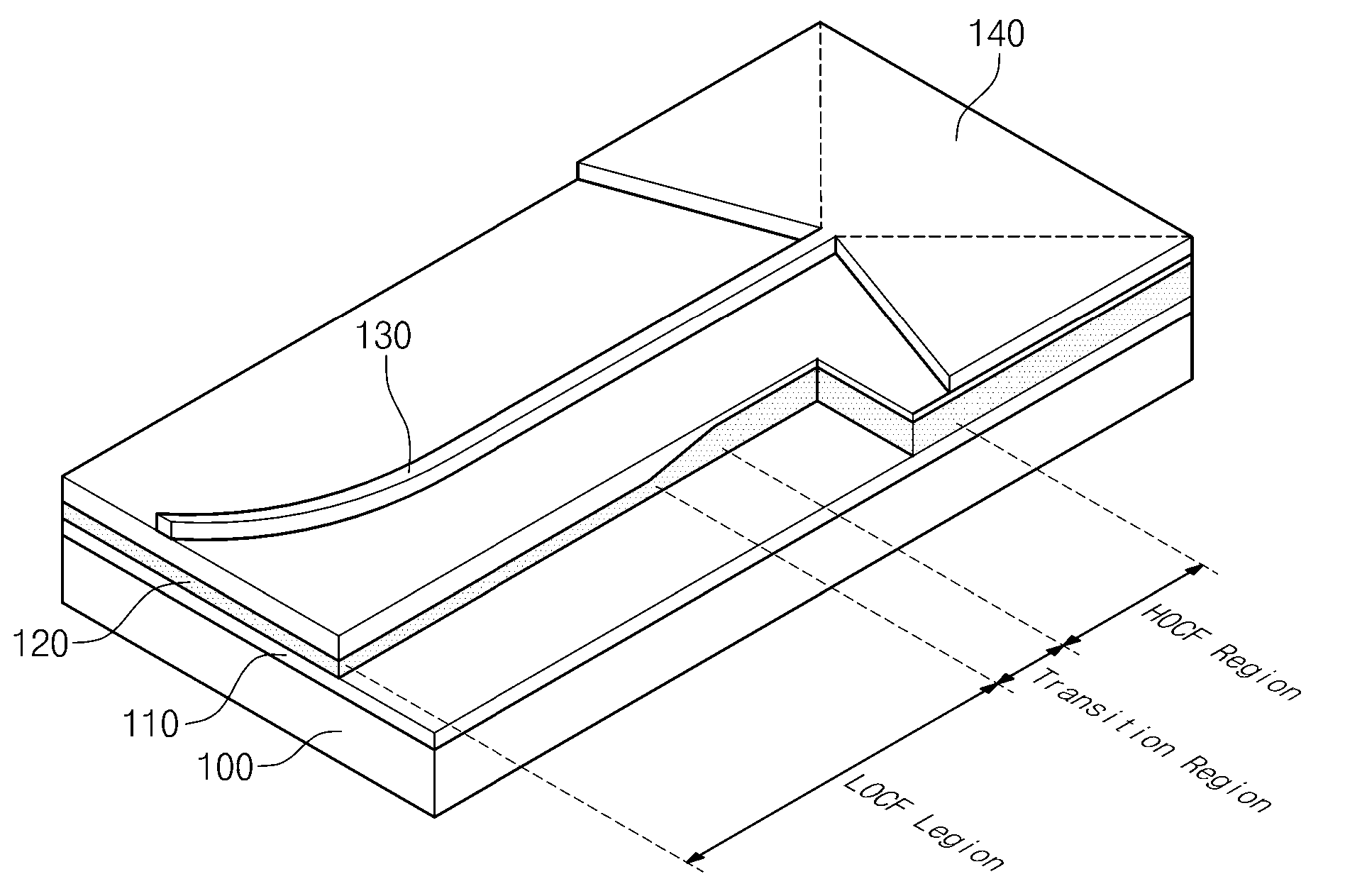
[0041]FIG. 1 is a perspective view of a superluminescent diode according to one embodiment of the present invention.

[0042]Referring to FIG. 1, the superluminescent diode according to one embodiment of the present invention includes a clad layer disposed on a substrate 100 and an active layer 120 inserted in the clad layer. The clad layer includes an n-type semiconductor layer 110 and a p-type semiconductor layer 130. The active layer 120 is interposed between the n-type and p-type semiconductor layers 110 and 130.

[0043]The active la...


PUM


Abstract

Provided are a superluminescent diode with a high optical power and a broad wavelength band, and a method of fabricating the same. The superluminescent diode includes: at least one high optical confinement factor (HOCF) region; and at least one low optical confinement factor (LOCF) region having a lower optical confinement factor than the HOCF region. The method includes obtaining a difference of optical confinement factors in the HOCF region and the LOCF region through a selective area growth method, the selective area growth method using a deposition thicknesses difference of thin layers according to a width difference of openings that expose a substrate.

Description

CROSS-REFERENCE TO RELATED APPLICATIONS[0001]This U.S. non-provisional patent application claims priority under 35 U.S.C. § 119 of Korean Patent Application No. 10-2007-0094558, filed on Sep. 18, 2007, the entire contents of which are hereby incorporated by reference.BACKGROUND OF THE INVENTION[0002]The present invention disclosed herein relates to an optoelectronic device and a method of fabricating the same, and more particularly, to a superluminescent diode with a high optical power and a broad wavelength band, and a method of fabricating the same.[0003]The present invention has been derived from research undertaken as a part of the information technology (IT) development business by Ministry of Information and Communication and Institute for Information Technology Advancement in the Republic of Korea (Project management No.: 2006-S-004-02, Project title: silicon based high speed optical interconnection IC).[0004]A superluminescent diode (SLD) is an optical device capable of prov...

Claims


Application Information

Patent Timeline
Patent Type & Authority Applications(United States)
IPC IPC(8): H01L29/06H01L21/02
CPCH01L33/02H01L33/0045H01L29/861
Inventor SONG, JUNG-HOKIM, KI-SOOLEEM, YOUNG-AHNKIM, GYUNG-OCK
Owner ELECTRONICS & TELECOMM RES INST
Learn More