Supercharge Your Innovation With Domain-Expert AI Agents!

Latchup robust array I/O using through wafer via

a technology of array i/o and wafer via, which is applied in the direction of semiconductor devices, electrical equipment, semiconductor/solid-state device details, etc., can solve the problems of destroying the integrated circuit in which latchup occurs, fets consuming large amounts of current overheating, and cmos field effect transistors (fets) in the circuits are susceptible to latch-up

Inactive Publication Date: 2009-06-18
IBM CORP
View PDF1 Cites 10 Cited by
  • Summary
  • Abstract
  • Description
  • Claims
  • Application Information

AI Technical Summary

Benefits of technology

[0003]A first aspect of the present invention is a structure, comprising: one or more logic circuits positioned in a region of a semiconductor substrate, the substrate having a top surface and a bottom surface, the one or logic circuits comprising first FETs having first well regions in the substrate, the first well regions extending from the top surface of the substrate into the substrate a first distance, the first distance less than whole distance between the top and bottom surfaces of the substrate; an I/O cell and an ESD protection device in the region of the substrate, the I/O cell comprising second FETs having second well regions in the substrate and the ESD protection device comprising third FETs having third well regions in the substrate, the second well regions extending from the top surface of the substrate into the substrate a second distance, the third well regions extending from the top surface of the substrate into the substrate a third distance, the second and third distances less than the whole distance; shallow trench isolation between the first, second and third FETs, the shallow trench isolation having a top surface coplanar with the top surface of the substrate and a opposite bottom surface in the substrate, the shallow trench isolation extending from the top surface of the substrate into the substrate a fourth distance, the fourth distance less than the whole distance; and an electrically conductive through via extending from the bottom surface of the substrate into the substrate a fifth distance, the fifth distance less than the whole distance, the through via abutting the bottom surface of shallow trench isolation between the ESD protection device and the I/O cell and at least one of the one or more logic circuits and intervening between the ESD protection device and the I/O cell and at least one of the one or more logic circuits.
[0004]A second a

Problems solved by technology

By placing I / O circuits in such close proximity to logic circuits, complementary metal-oxide-silicon (CMOS) field effect transistors (FETs) in the circuits have been found to be susceptible to latch-up.
Latch-up causes FETs to consume large amounts of current overheating and destroying the integrated circuit in which latchup occurs.
Existing methods for reducing this propensity to latchup have become increasingly less effective as doping levels of the substrates of integrated circuits have decreased.

Method used


Image

  • Latchup robust array I/O using through wafer via
  • Latchup robust array I/O using through wafer via
  • Latchup robust array I/O using through wafer via

Examples


first embodiment

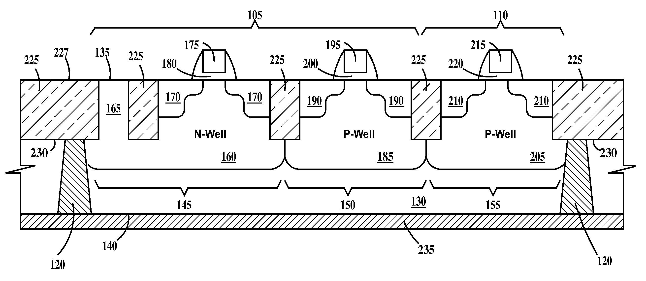
[0015]FIG. 2 is a cross-section through line 2 / 3-2 / 3 of FIG. 1 illustrating the present invention. In FIG. 2, a substrate 130 has a top surface 135 and a bottom surface 140. An exemplary I / O cell 105 includes a P-channel FET (PFET) 145 and an N-channel FET (NFET) 150 by way of example. There may be other FETs in I / O cell 105. An exemplary ESD protection device 110 includes an NFET 155 by way of example. Other examples of devices that may be used for ESD protection device 110 include PFETs, other Metal-Oxide-Silicon FETS (MOSFETS), bipolar transistors, resistors, diffused capacitors, N+ diffusions, and n-well to substrate diodes. There may be additional FETs in ESD protection device 155. In one example, ESD protection device 110 may include any device capable of injecting current into substrate 100. PFET 145 includes an N-Well 160 formed in substrate 130, an N-Well contact 165 and source / drains 170 formed in the N-Well. A gate electrode 175 is formed over a channel region of the N-We...

second embodiment

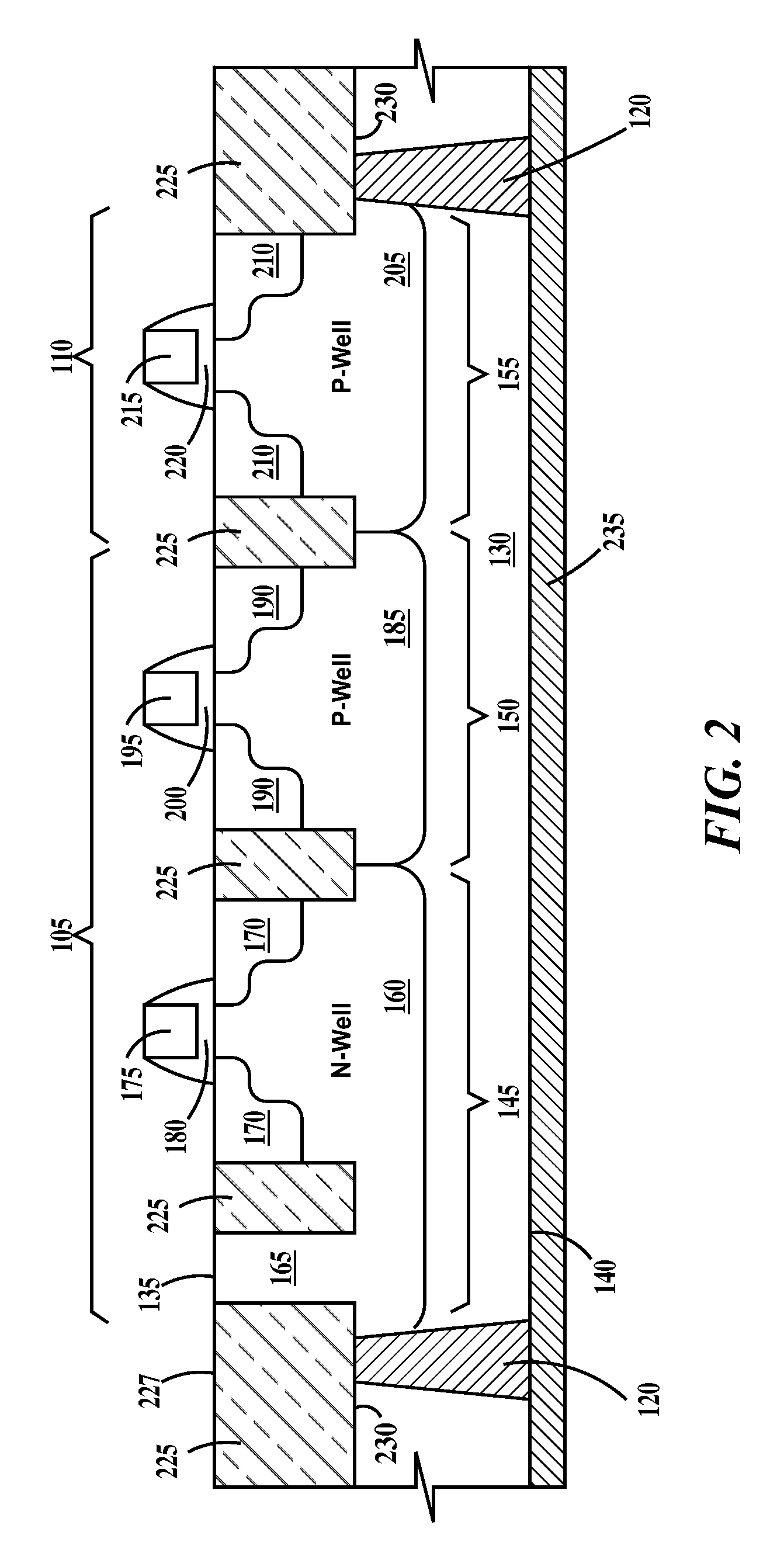
[0019]FIG. 3 is a cross-section through line 2 / 3-2 / 3 of FIG. 1 illustrating the present invention. FIG. 3 differs from FIG. 2 only in through via 120 is not abutting N-Well 160 or P-Well 205. A region 240 of substrate 130 intervenes between through via 120 and N-Well 160 and P-Well 205. Region 240 may form a depletion region during operation of the integrated circuit chip.

third embodiment

[0020]In the present invention, some regions of through vias 120 abut N-Wells and / or P-Wells as illustrated in FIG. 2 and some regions of through vias 120 do not abut N-Wells and / or P-Wells as illustrated in FIG. 3.

[0021]Thus, the embodiments of the present invention provide more robust latchup preventive structures and methods for preventing latchup in integrated circuits having I / Os embedded in the core circuit regions of integrated circuit chips.


PUM


Abstract

A structure and a method for preventing latchup. The structure including: an I / O cell and an ESD protection circuit in a region of an integrated circuit chip containing logic circuits; an electrically conductive through via extending from a bottom surface of the substrate toward a top surface of the substrate between the I / O cell and an ESD protection circuit and at least one of the logic circuits.

Description

FIELD OF THE INVENTION[0001]The present invention relates to the field of Integrated circuits; more specifically, it relates to an array I / O structure and method of making array I / O latchup robust.BACKGROUND OF THE INVENTION[0002]In modern integrated circuits, input / output (I / O) circuits are placed within a region of the integrated circuit chip containing logic circuits. By placing I / O circuits in such close proximity to logic circuits, complementary metal-oxide-silicon (CMOS) field effect transistors (FETs) in the circuits have been found to be susceptible to latch-up. Latch-up causes FETs to consume large amounts of current overheating and destroying the integrated circuit in which latchup occurs. Existing methods for reducing this propensity to latchup have become increasingly less effective as doping levels of the substrates of integrated circuits have decreased. Therefore there is a need in the industry for more robust latchup preventive structures and methods for preventing la...

Claims


Application Information

Patent Timeline
IPC IPC(8): H01L27/06H01L21/8234
CPCH01L27/0251H01L27/0921H01L2924/0002H01L2924/00
Inventor CHAPMAN, PHILLIP FRANCISCOLLINS, DAVID S.VOLDMAN, STEVEN H.
Owner IBM CORP
Features
  • R&D
  • Intellectual Property
  • Life Sciences
  • Materials
  • Tech Scout
  • Unparalleled Data Quality
  • Higher Quality Content
  • 60% Fewer Hallucinations
Learn More