Magnetic head and magnetic recording apparatus

a magnetic recording and head technology, applied in the field of magnetic recording apparatuses, can solve the problems of difficult to apply the medium of 1 tbit/insup>2 /sup>or more in respect of resolving power, and the output of conventional spin accumulation elements is not enough

Active Publication Date: 2009-06-18
WESTERN DIGITAL TECH INC
View PDF9 Cites 27 Cited by
  • Summary
  • Abstract
  • Description
  • Claims
  • Application Information

AI Technical Summary

Benefits of technology

[0043]FIG. 10 shows the magnetic electrode distance dependency of the output signal of the fifth spin accumulation element according to the invention. The solid line represents the output voltage of the fifth spin accumulation element according to an embodiment of the invention, and the broken line represents the output voltage of the spin accumulation element having the single spin injection part. In the fifth spin accumulation element, assuming that the line width of the non-magnetic conductor 1 is wN, the film thickness is tN, the line width of the second spin injection part in a direction perpendicular to the fine line direction of the non-magnetic conductor 1 is wSH, the spin polarizability on the interface between the first spin injection part 10 and the non-magnetic conductor 1 is Pi, the spin polarizability of the detection part on the interface between the magnetic conductor 6 and the non-magnetic conductor 1 is Pd, the spin diffusion length of the non-magnetic conductor 1 is λN, the resistivity of the non-magnetic conductor 1 is ρN, the resistivity of the second spin injection part is ρSH, the spin Hall coefficient of the second spin injection part is αSH, and the distance between the first magnetic conductor 3 and the magnetic conductor 6 is d1, the output voltage owing to the spin accumulation effect in the reversible spin Hall effect can be represented in the form of:
[0044]FIGS. 11(a)-11(d) are typical views of the reproducing head having the fifth spin accumulation element. FIG. 11(a) is a perspective view of the reproducing head, and FIGS. 11(b), 11(c) and 11(d) show the cross sections taken along BB′, CC′ and DD′.
[0045]The spin injection part of the reproducing head has a structure in which the current terminal 15, the contact 13, the non-magnetic conductor 1, the first spin injection part 10, the buffer layer 14, and the top shield 17 are laminated successively, and the second spin injection part 12 is electrically joined with the non-magnetic conductor 1, as shown in FIG. 11(c). It is assumed that the currents flowing through the first spin injection part 10 and the second spin injection part are Ic1 and Ic2, and the current terminal is common to the top electrode 18 and the electrode terminal 15. The non-magnetic conductor making up the second spin injection part 12 is connected with the electrode terminal 15 and the top shield 17 via the contact 13. A detection part of leakage flux, which is shown in FIG. 11(d), has a structure in which the bottom shield 18, the contact 13, the non-magnetic conductor 1, the tunneling junction 5, the magnetic conductor 6, the voltage terminal 16, and the top shield 17 are laminated successively. The voltage terminal 16 is electrically insulated from the top shield 17, and detects the output voltage between the voltage terminal 16 and the bottom shield 18.
[0046]FIG. 12 is a typical view of a magnetic head 40 that is combined with a laminated recording head 42 and uses as a reproducing head 41 the spin accumulation element having a plurality of spin injection parts according to the invention. Though the spin accumulation element as shown is the first spin accumulation element of an embodiment of the invention, the spin accumulation element of an embodiment the invention having the other structure may be employed.
[0047]FIG. 13 is a typical view of a magnetic recording apparatus according to an embodiment of the invention. This magnetic recording apparatus comprises a magnetic recording medium 52 having a magnetic recording layer, a drive section 54 for driving the magnetic recording medium, the magnetic head 40 according to an embodiment of the invention for performing the recording and reproducing operation on and from the magnetic recording medium, an actuator 50 and a slider 51 for moving the magnetic head to a predetermined position on the magnetic recording medium, and means for processing the output signal from the magnetic head. The magnetic recording medium such as a longitudinal recording continuous medium, a perpendicular recording continuous medium, a discrete medium or a pattern medium may be employed.

Problems solved by technology

However, for these heads, it may be difficult to make the gap length Gw between shields 30 nm or less due to the requirements for the film thickness of an element, and difficult to apply them to the medium of 1 Tbit / in2 or more in respect of the resolving power.
However, the conventional spin accumulation element does not have enough output, and is required to have the higher output.
However, with the present micro fabrication technique, the magnetic substance interval is about 30 nm at minimum, and impossible to narrow down to infinitesimal.
Also, if the magnetic substance interval distance is smaller, a magnetic interaction acts between two magnetic substances, possibly degrading the magnetic characteristics.

Method used


Image

  • Magnetic head and magnetic recording apparatus
  • Magnetic head and magnetic recording apparatus
  • Magnetic head and magnetic recording apparatus

Examples


example 1

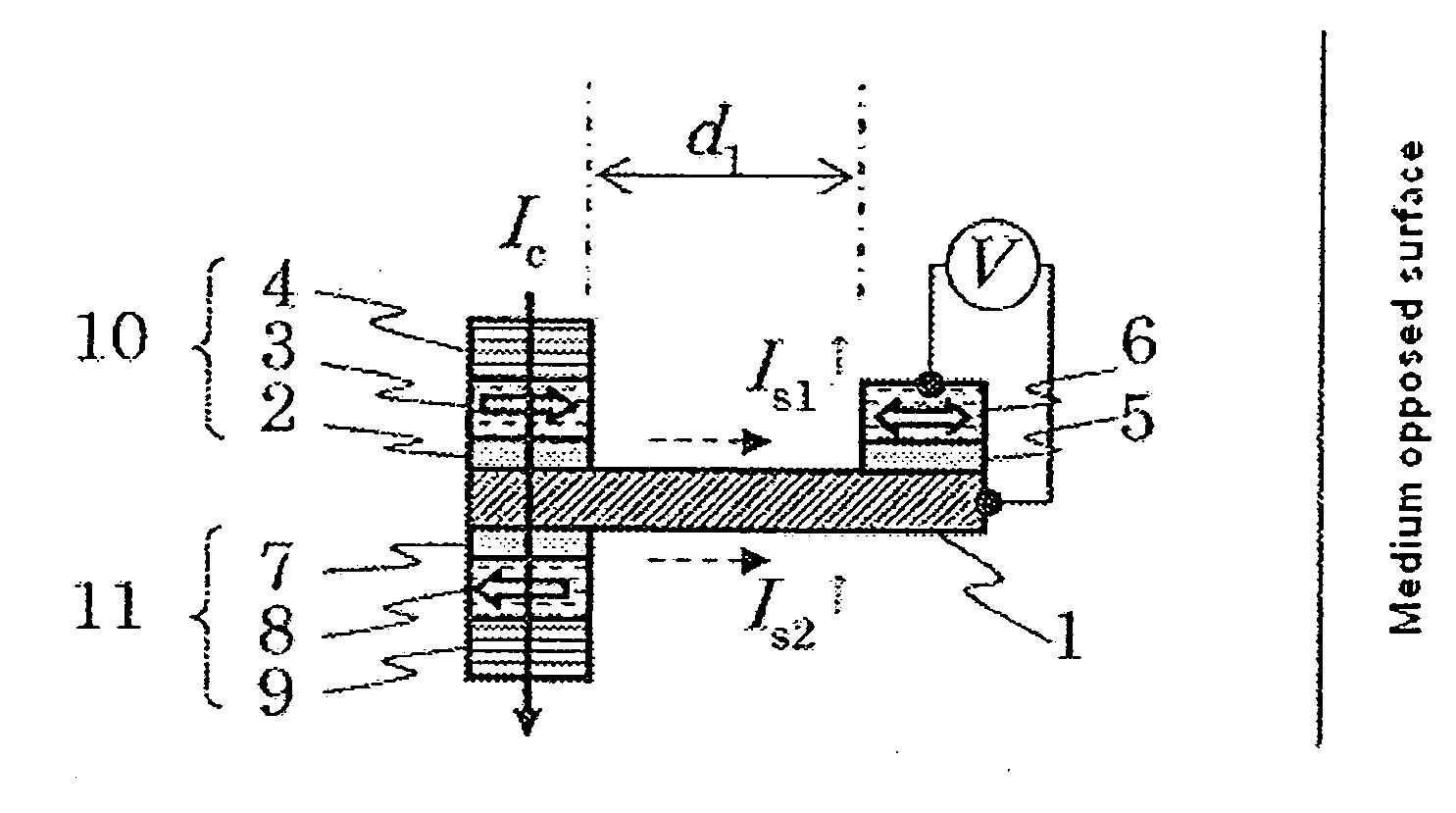
[0048]To verify the effect of the first spin injection element of the invention as shown in FIGS. 1 and 7(a)-7(d), two kinds of spin accumulation element were fabricated. For the first spin accumulation element, the material of the non-magnetic conductor 1 was Al. The Al fine line as used in the example 1 had a line width wN of 100 nm, a film thickness tN of 10 nm, and a length LN of 3 μm, with the electrical resistivity ρN being 2.5 μΩcm. An Al—Ox barrier layer was employed as the first tunneling junction 2, the second tunneling junction 7 and the third tunneling junction 5. The Al—Ox barrier was formed by naturally oxidizing the surface of the Al fine line. Co having a film thickness of 10 nm was employed as the first magnetic conductor 3, the second magnetic conductor 8 and the third magnetic conductor 6. The line width wco1, wco2 of the first magnetic conductor Co1 and the second magnetic conductor Co2 was 200 nm, and the line width wco3 of the third magnetic conductor Co3 was 1...

example 2

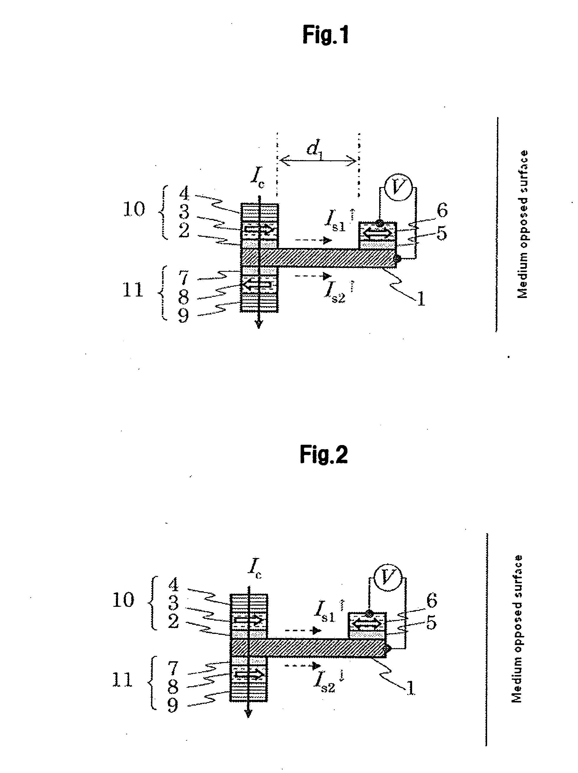
[0051]In the example 2, the fourth spin accumulation element of an embodiment of the invention was fabricated as shown in FIG. 4(a). The material and size of the element were the same as in the example 1, except that the second spin injection part 12 was provided on the non-magnetic conductor 1 on the same side of the first spin injection part 11 with a spacing from it, as shown in FIG. 4(a). Assuming that the interval distance between the first spin injection part 10 and the second spin injection part 11 was Δd (=d2−d1), three kinds of Δd=100, 300 and 500 nm were prepared, whereby the non-local measurement was conducted in the range of 30 nm≦d1≦1000 nm. A magnetic field was applied in parallel to the fine line direction of the non-magnetic conductor 1.

[0052]FIG. 6 shows the electrode distance d1 dependency of the output voltage ΔV in the case of Δd=100, 300 and 500 nm in the fourth spin accumulation element of an embodiment of the invention. For comparison, the result of the conven...

example 3

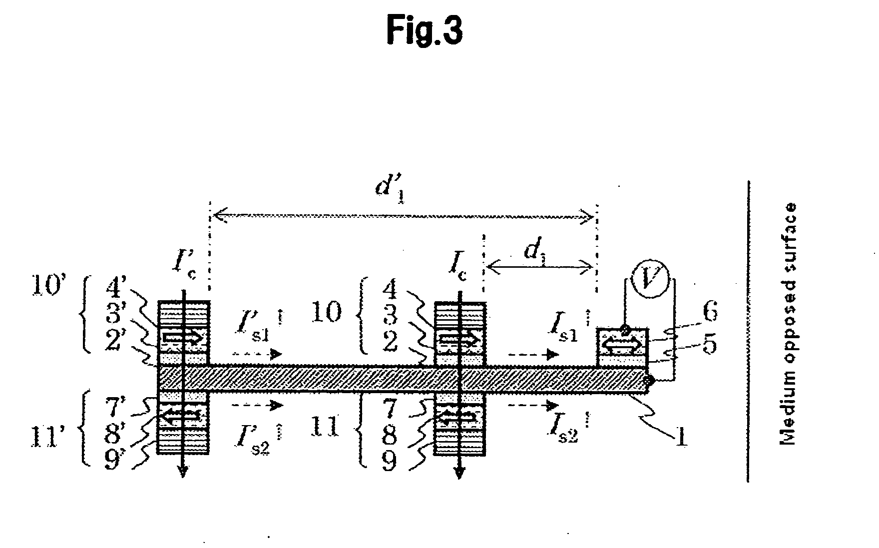
[0053]In the example 3, the fifth spin injection element of the invention was fabricated as shown in FIGS. 9(a)-9(c) and FIGS. 11(a)-11(d). The non-magnetic conductor 1 as employed in the example 3 was the Al fine line having the size of the line width wN=100 nm, the film thickness tN=10 nm, and the length LN=3 μm, with the electrical resistivity ρN being 2.5 μΩcm. An Al—Ox barrier layer that was produced by naturally oxidizing the surface of Al was employed as the tunneling junctions 2 and 5 as shown in FIGS. 9(a)-9(c). Co having a film thickness of 10 nm was employed as the first magnetic conductor 3 and the third magnetic conductor 6. The line width of the first magnetic conductor Co1 was wco1=200 nm and the line width of the third magnetic conductor Co3 was wco3=100 nm. The magnetization of Co1 was fixed in one direction by the antiferromagnetic conductor MnIr having a film thickness of 10 nm, and the distance between Co1 and Co3 was narrowed down to d1=30 nm at minimum. On the ...


PUM

PropertyMeasurementUnit
thicknessaaaaaaaaaa
magnetizationaaaaaaaaaa
external magnetic fieldaaaaaaaaaa

Abstract

Embodiments of the present invention provide an accumulation element with high resolving power and high output suitable for magnetic recording and reproducing at high recording density. According to one embodiment, a plurality of spin injection parts and are provided to increase the total amount of spin electrons. The spin accumulation element is composed of a non-magnetic conductor, a first magnetic conductor, a second magnetic conductor, and a third magnetic conductor, each of which are in contact with the non-magnetic conductor through the tunneling junction. An output voltage due to the spin accumulation effect is detected as a potential difference between the non-magnetic conductor and the third magnetic conductor. The first magnetic conductor of the first spin injection part is fixed by a first antiferromagnetic conductor and the second magnetic conductor of the second spin injection part is fixed by a second antiferromagnetic conductor so that their directions of magnetization are anti-parallel to each other.

Description

CROSS-REFERENCE TO RELATED APPLICATION[0001]The instant nonprovisional patent application claims priority to Japanese Patent Application No. 2007-323468 filed Dec. 14, 2007 and which is incorporated by reference in its entirety herein for all purposes.BACKGROUND OF THE INVENTION[0002]The recording density of a magnetic recording / reproducing apparatus has been increasing at an annual rate from 40 to 60%, and is estimated to reach Tbit / in2 in the near future. Accordingly, it is required that a magnetic recording / reproducing head has higher output and higher resolving power. Presently, the magnetic reproducing heads such as a CPP-GMR (Current Perpendicular to Plane Giant Magneto Resistance) head in which a sense current is passed perpendicularly to the laminated plane, and a TMR (Tunneling Magneto Resistance) head, have been proposed. However, for these heads, it may be difficult to make the gap length Gw between shields 30 nm or less due to the requirements for the film thickness of a...

Claims


Application Information

Patent Timeline
Patent Type & Authority Applications(United States)
IPC IPC(8): G11B5/33
CPCB82Y25/00G11B5/332G01R33/1284G01R33/093G11B5/3909
Inventor YAMADA, MASAKITAKAHASHI, HIROMASA
Owner WESTERN DIGITAL TECH INC
Why Eureka
Try Eureka