

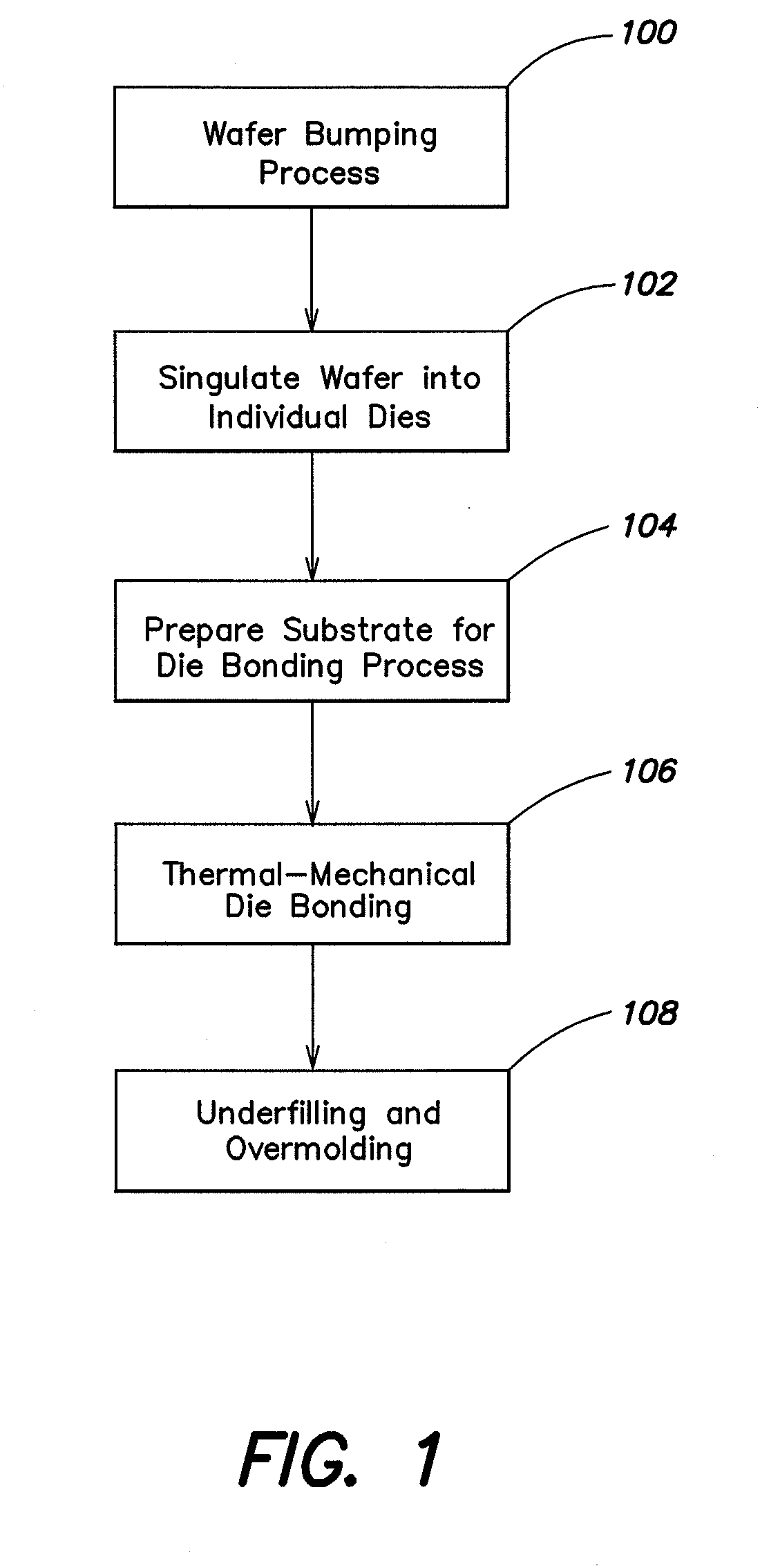
Thermal mechanical flip chip die bonding
a flip chip and die bonding technology, applied in semiconductor/solid-state device testing/measurement, semiconductor devices, semiconductor/solid-state device details, etc., can solve the problems of increasing the cost of component manufacturing, gold bumping is an expensive material, and gold bumping (and providing substrates with gold bond pads) is far more expensive than solder bumping, so as to achieve good bond strength and electrical performance.
- Summary
- Abstract
- Description
- Claims
- Application Information
AI Technical Summary
Benefits of technology
Problems solved by technology
Method used
Image

Examples
Embodiment Construction
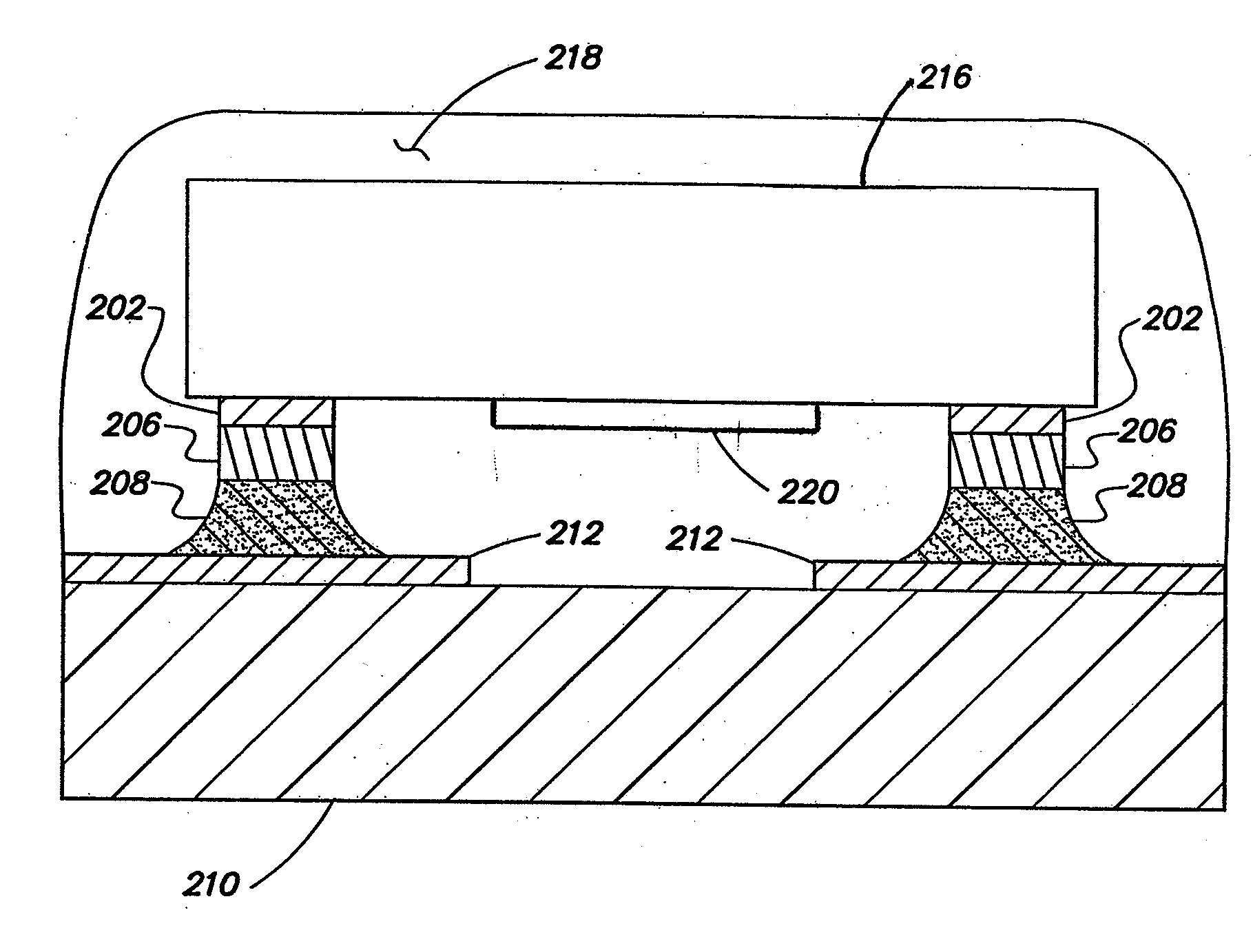
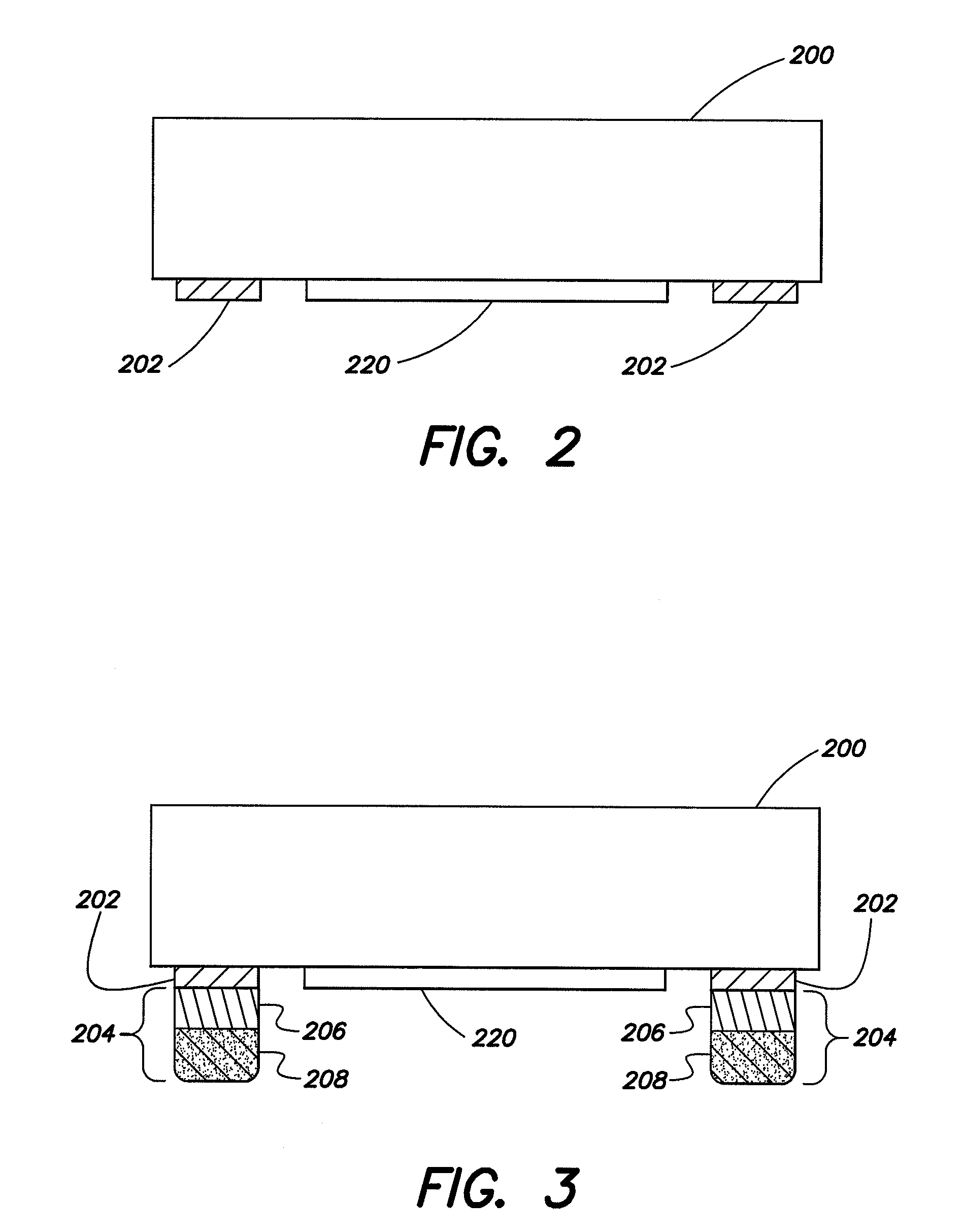
[0021]At least some aspects and embodiments are directed to flip chip die bonding techniques and processes, and devices made according to the same. As discussed above, conventional flip chip to substrate interconnection copper-tin bonding methods require multi-step assembly processes, which are undesirable. Although gold-to-gold interconnect (GGI) processes may be simpler and cleaner, gold is expensive and it may therefore, often be undesirable to use gold-bumped dies. According to at least some aspects of the invention, a flip chip bonding method may include a thermosonic die bonding process in which thermal and ultrasonic energy may be applied, under pressure, to achieve a bond between a copper pillar bump on a wafer and a conductive pad of a substrate. As discussed above, thermosonic bonding is used in GGI bonders to form pure gold bonds between gold-bumped dies and the gold pads of a substrate. However, these gold bolds are homogenous, and gold is known to be a soft, malleable m...
PUM
 Abstract
Description
Claims
Application Information