

Electro-optical device and electronic apparatus
a technology of optical devices and electronic devices, applied in the direction of instruments, electric digital data processing, computing, etc., can solve the problems of low aperture ratio, difficulty in satisfactorily performing both display and sensing, and lowering the aperture ratio of a display area, so as to achieve the effect of increasing sensing performance and lowering display performan
- Summary
- Abstract
- Description
- Claims
- Application Information
AI Technical Summary
Benefits of technology
Problems solved by technology
Method used
Image

Examples
first embodiment
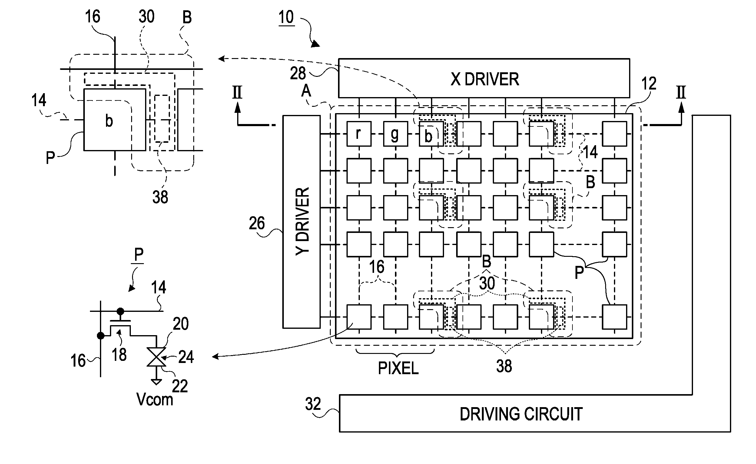
[0033]FIG. 1 is a block diagram showing the configuration of a liquid crystal display as an electro-optical device according to this embodiment. A liquid crystal display 10 has a display area A, and a plurality of sensing areas B that are provided in the display area A. The sensing areas B overlap a black matrix (BM) 12 that is a non-display area where no image is displayed. Provided in the display area A are a plurality of scanning lines 14, a plurality of data lines 16, and a plurality of pixel circuits P that are planarly provided at intersections of the scanning lines 14 and data lines 16 with the BM 12 in the vicinity thereof. Each of the pixel circuits P includes a transistor 18, a pixel electrode 20, a common electrode 22, to which a common potential Vcom is applied, and a liquid crystal layer 24 that is interposed between the pixel electrode 20 and the common electrode 22. The transistor 18 is formed of a TFT (Thin Film Transistor) element. A gate of the transistor 18 is con...
second embodiment
[0056]A second embodiment will be described with reference to the drawings.
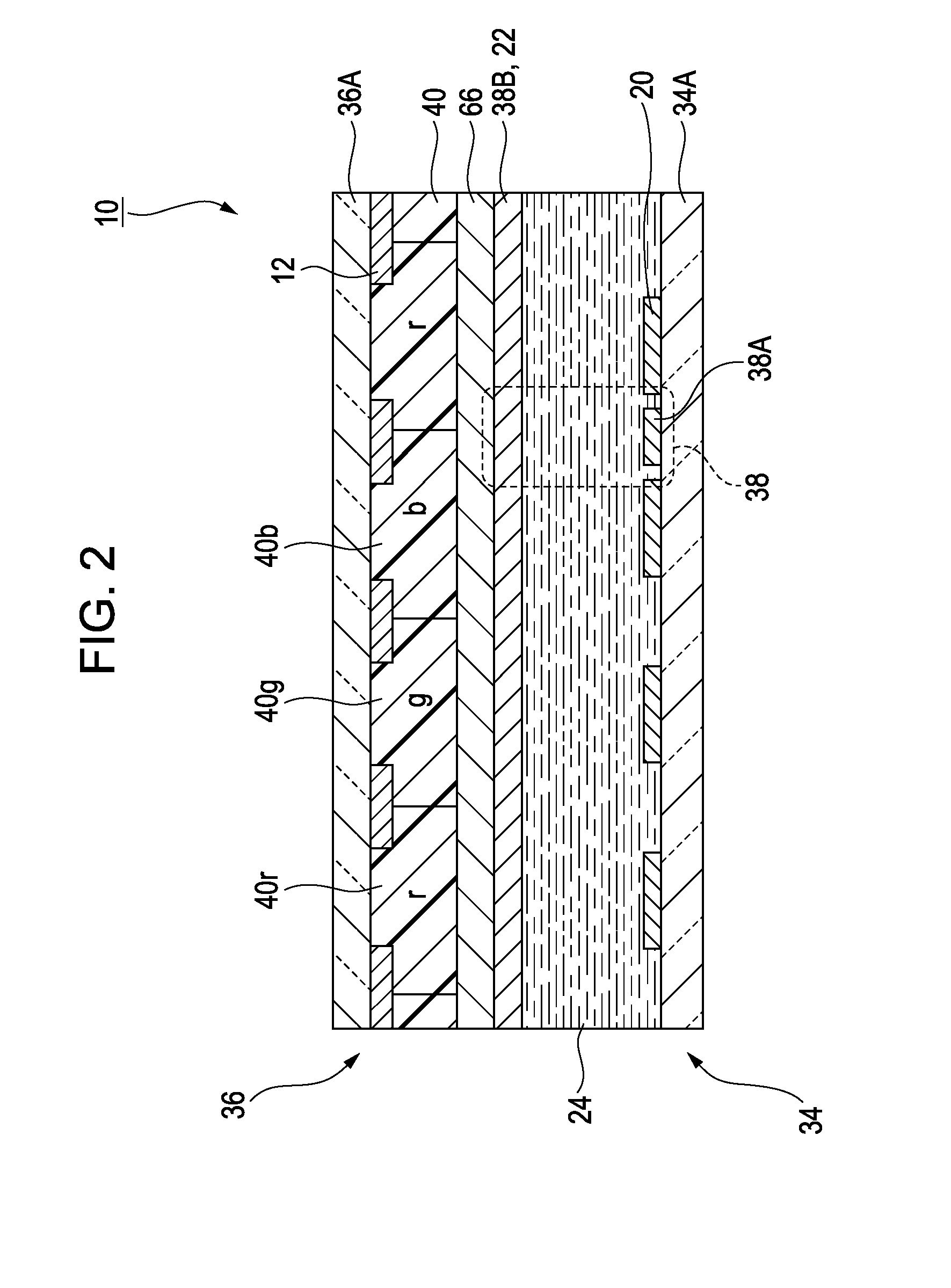
[0057]FIG. 9 is a schematic sectional view showing the structure of a liquid crystal display according to this embodiment, which includes a capacitance detection element 38. Similarly to the liquid crystal display 10 of the first embodiment, a liquid crystal display 64 of this embodiment is a TFT active driving transmissive liquid crystal display. The liquid crystal display 64 is characterized by a gap between the first electrode 38A and the second electrode 38B. The liquid crystal display of this embodiment has the same basic configuration as that of the liquid crystal display of the first embodiment. Therefore, the same parts are represented by the same reference numerals, and thus description thereof will be omitted.
[0058]As shown in FIG. 9, in the liquid crystal display 64 of this embodiment, a protrusion 68 is provided at a portion of the second electrode 38B opposing the first electrode 38A (a portion o...
third embodiment
[0059]Next, a third embodiment will be described with reference to the drawings. As shown in FIG. 1, in a liquid crystal display 10 of this embodiment, at least two of a plurality of capacitance detection elements 38 are electrically connected in parallel. With this configuration, an overlap area of the opposing electrodes of the capacitance detection element 38 increases, and a capacitive component increases. Therefore, it is possible to improve sensing performance without lowering display quality.
Electronic Apparatus
[0060]Next, an electronic apparatus using a liquid crystal display according to the foregoing embodiment will be described with reference to FIGS. 10A to 10C.
[0061]FIG. 10A is a perspective view showing the configuration of a mobile personal computer 100, which uses the liquid crystal display 10 (64) of the foregoing embodiment as a display unit. The personal computer 100 has the liquid crystal display 10 (64) as a display unit, and a main body 102. In the main body 10...
PUM
 Abstract
Description
Claims
Application Information