Immersion lithography wafer edge bead removal for wafer and scanner defect prevention

a technology of scanning and lithography, applied in the field of integrated circuits, can solve the problems of affecting the processing speed of ebr, affecting the quality of lithography, and affecting the quality of lithography, and achieve the effect of reducing the generation of contamination

Active Publication Date: 2009-06-25
TEXAS INSTR INC
View PDF5 Cites 11 Cited by
  • Summary
  • Abstract
  • Description
  • Claims
  • Application Information

AI Technical Summary

Benefits of technology

[0005]An advantage of the instant invention is a reduction in particulate contamination compared to other methods of forming a layered stack of photolithographic materials for immersion lithography.

Problems solved by technology

Immersion lithographic processing exacerbates the problem because the immersion fluid picks up fragments of layer material as it passes over the wafer edge, causing pattern defects and particulate contamination.
EBR processes are hampered by adhesion incompatibilities between top coat materials and BARC materials.
Furthermore, repeated EBR processes can damage BARC layers, resulting in additional particulates.

Method used


Image

  • Immersion lithography wafer edge bead removal for wafer and scanner defect prevention
  • Immersion lithography wafer edge bead removal for wafer and scanner defect prevention
  • Immersion lithography wafer edge bead removal for wafer and scanner defect prevention

Examples


first embodiment

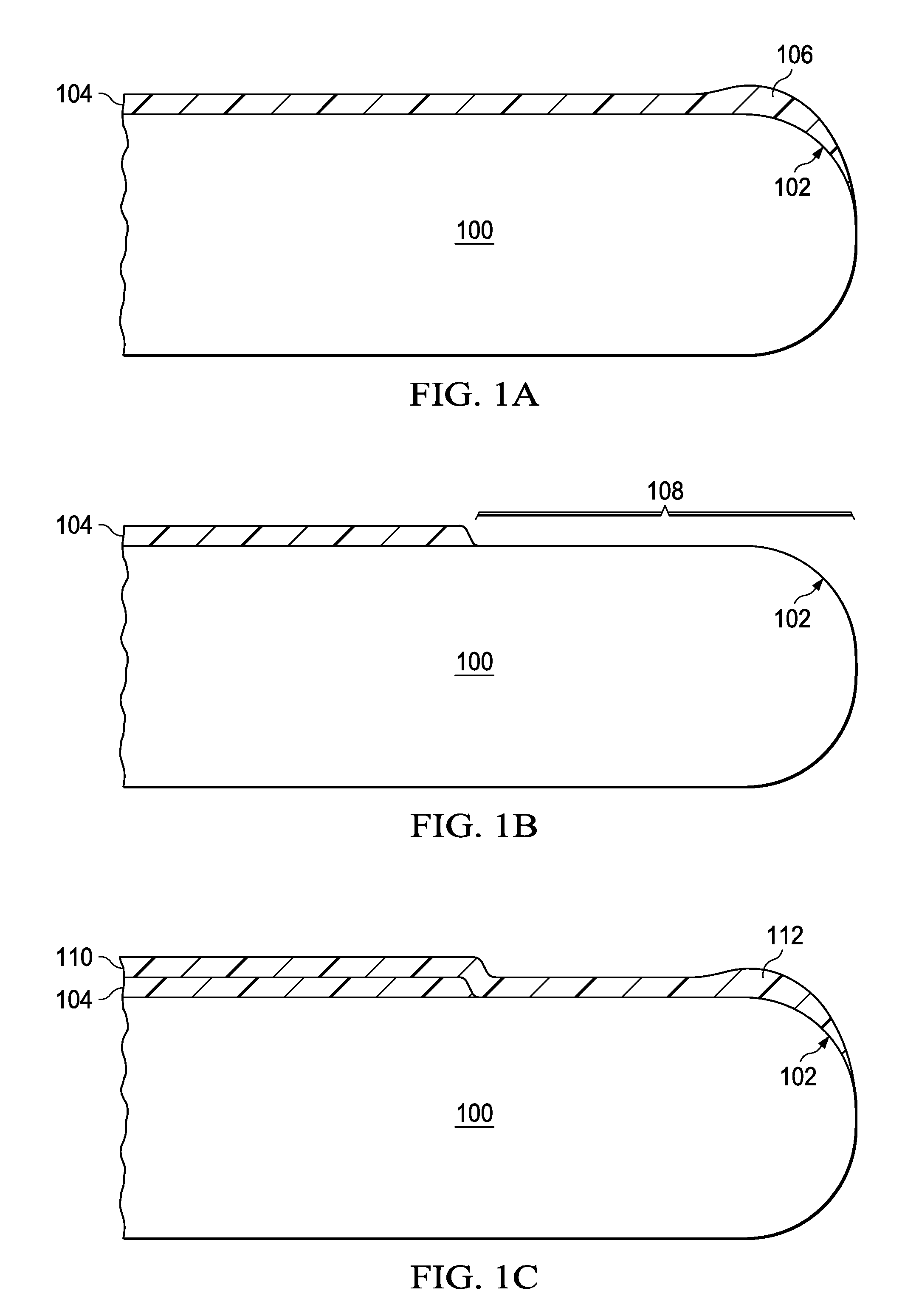
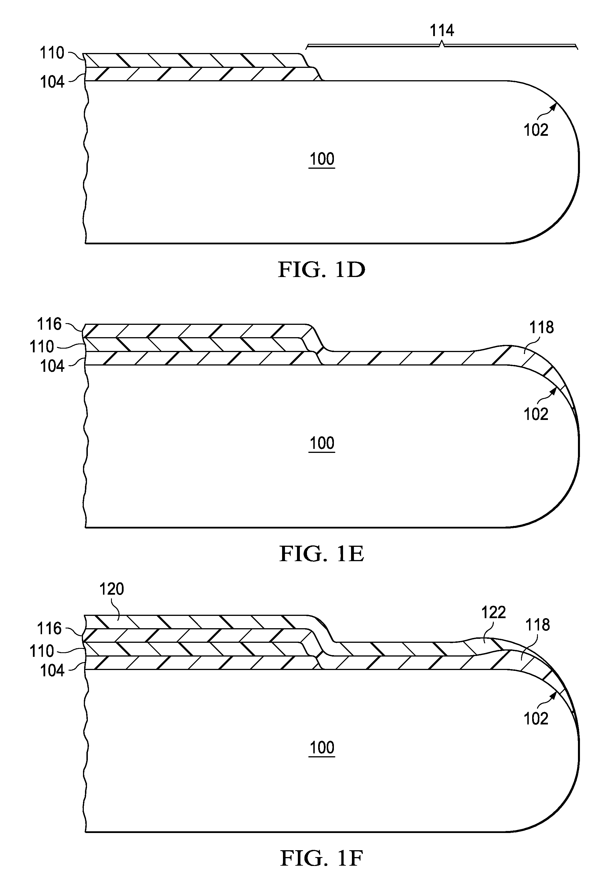
[0011]FIG. 1A through FIG. 1G are cross-sections of a wafer edge during formation of a photolithographic layer stack according to the instant invention. FIG. 1A depicts a wafer (100) with an edge region (102) having a radius between 100 and 350 microns. A first BARC layer (104) of a first BARC material is formed on a top surface of the wafer (100), typically by dispensing a measured amount of fluid containing the first BARC material diluted by a first solvent onto the wafer (100) followed by spinning the wafer (100) at several hundred to several thousand rpm while a portion of the first solvent evaporates from the BARC fluid, producing the first BARC layer (104) and a first BARC edge bead (106) along the wafer edge region (102). A composition of the first BARC material and a thickness of the first BARC layer (104) depends on the particular pattern being formed during fabrication of an integrated circuit on the wafer (100), and may be substantially organic, with optional light absorb...

second embodiment

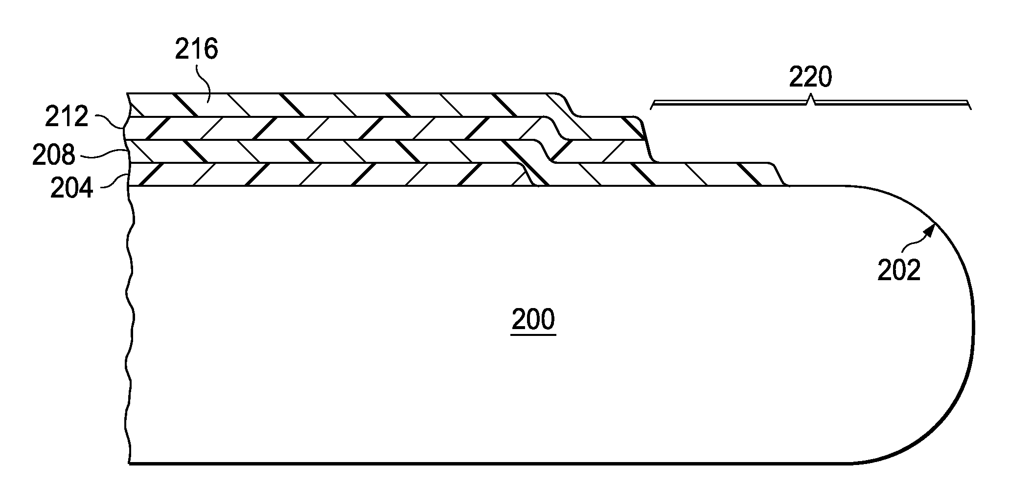
[0019]FIG. 2A through FIG. 2D are cross-sections of a wafer edge during formation of a photolithographic layer stack according to the instant invention. FIG. 2A depicts a wafer (200) with an edge region (202) having a radius between 100 and 350 microns. A first BARC layer (204) of a first BARC material is formed on a top surface of the wafer (200), typically by dispensing a measured amount of fluid containing the first BARC material diluted by a first solvent onto the wafer (200) followed by spinning the wafer (200) at several hundred to several thousand rpm while a portion of the first solvent evaporates from the BARC fluid, producing the first BARC layer (204) and a first BARC edge bead along the wafer edge region (202). A composition of the first BARC material and a thickness of the first BARC layer (204) depends on the particular pattern being formed during fabrication of an integrated circuit on the wafer (200), and may be substantially organic, with optional light absorbing dy...


PUM

PropertyMeasurementUnit
radiusaaaaaaaaaa
radiusaaaaaaaaaa
thicknessaaaaaaaaaa

Abstract

A method of performing a single step / single solvent edge bead removal (EBR) process on a photolithography layer stack including a photoresist layer and a top coat layer using propylene glycol monomethyl ether acetate (PGMEA) or a mixture of PGMEA and gamma-butyrolactone (GBL) is disclosed. The single step / single solvent EBR process is compatible with organic and inorganic BARC layers.

Description

FIELD OF THE INVENTION[0001]This invention relates to the field of integrated circuits. More particularly, this invention relates to methods to improve immersion lithography processes used to fabricate integrated circuits.BACKGROUND OF THE INVENTION[0002]Immersion lithography, in which a liquid, known as an immersion fluid, is inserted between the lens and the wafer, is used to define patterns on some advanced integrated circuits. Typical immersion photolithography processes use a stack of multiple layers of materials, including a bottom anti-reflection coating, commonly known as BARC, an optional second BARC layer, a photoresist layer, and a top coat which reduces reflections, and optionally reduces friction between the wafer and the immersion fluid during wafer movement and / or provides a barrier between the immersion liquid and the photoresist, sometimes called TARC (top anti-reflection coating). These layers are typically applied by spin coating, which produces an edge bead of la...

Claims


Application Information

Patent Timeline
Patent Type & Authority Applications(United States)
IPC IPC(8): H01L21/306
CPCH01L21/0271H01L21/02087
Inventor RATHSACK, BENJAMEN MICHAELSOMERVELL, MARK HOWELL
Owner TEXAS INSTR INC
Why Eureka
Try Eureka