

System and method for routing connections
a routing connection and routing method technology, applied in the field of electronic circuit can solve the problems that the evolution of electronic design automation (eda) tools has not kept pace with the increase in performance demands, and achieve the effects of optimizing wire spacing, increasing device performance, and minimal size increases
- Summary
- Abstract
- Description
- Claims
- Application Information
AI Technical Summary
Benefits of technology
Problems solved by technology
Method used
Image

Examples
Embodiment Construction
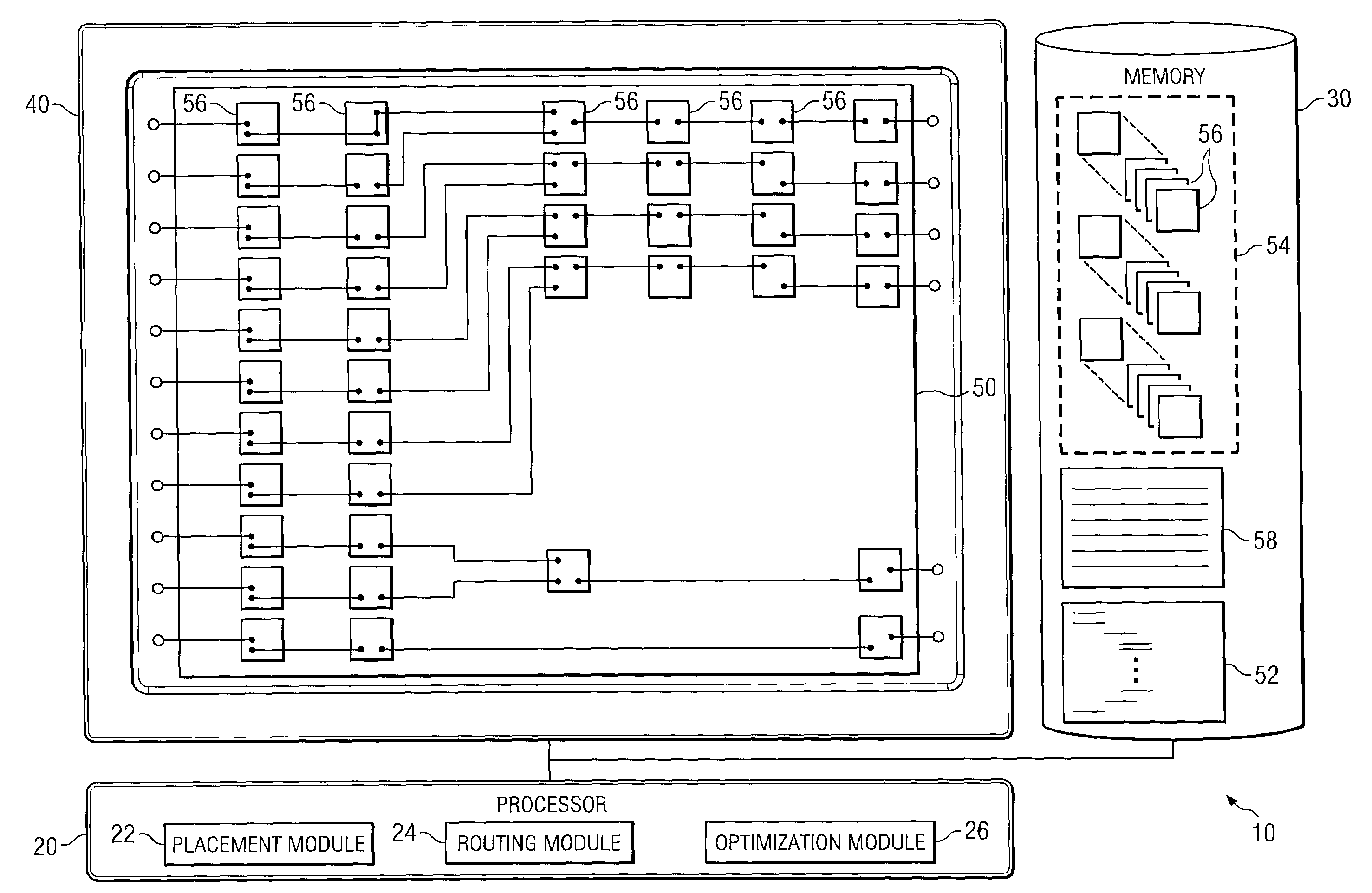
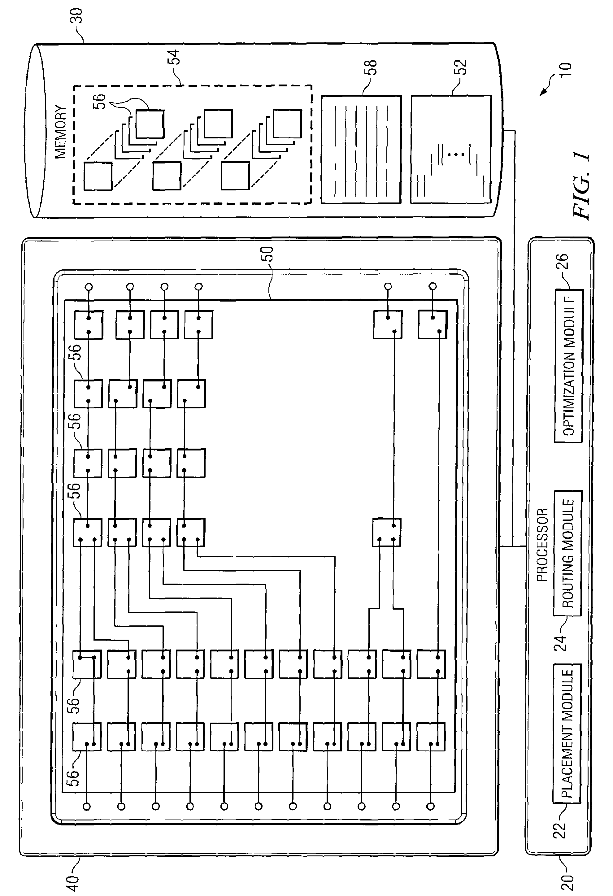
[0013]FIG. 1A illustrates a system 10 for designing integrated electronic circuits. In the illustrated embodiment, system 10 includes a processor 20, a memory 30, and a display 40. Additionally, in particular embodiments, system 10 includes a plurality of modules capable of performing certain tasks related to the design, modeling, and / or simulation of electronic circuits, such as a placement module 22, a routing module 24, and an optimization module 26. In particular embodiments, system 10 may improve the performance of electronic circuits designed with system 10 by optimizing interconnect elements within the electronic circuits.
[0014]More specifically, in particular embodiments, the electronic circuits designed by or using system 10 include a plurality of circuit elements that are connected by a collection of wires to facilitate predetermined functionality in the relevant electronic circuit. By optimizing the spacing of these wires, as described further below, system 10 may reduce ...
PUM
 Abstract
Description
Claims
Application Information