Photoelectric conversion device and manufacturing method thereof

Inactive Publication Date: 2009-07-02
SEMICON ENERGY LAB CO LTD
View PDF102 Cites 58 Cited by
  • Summary
  • Abstract
  • Description
  • Claims
  • Application Information

AI Technical Summary

Benefits of technology

[0016]In accordance with the present invention, a surface portion of a single crystal semiconductor substrate is thinned and bonded to a supporting substrate, whereby a photoelectric conversion device in which a top cell is stacked over a bottom cell can be obtained. The bottom cell uses a single crystal semiconductor layer with a thickness of 10 μm or less as a photoelectric conversion layer, and the top cell uses a layer including an organic semiconductor material as a photoelectric conversion layer. That is, a photoelectric conversion device can be manufactured in which a bottom cell using a single crystal semiconductor layer as a photoelectric conversion layer and a top cell which uses a layer including an organic semiconductor material as a photoelectric conversion layer and is stacked over the bottom cell, are provided over a

Problems solved by technology

However, a crystalline silicon thin-film solar cell is still inferior to a single crystal silicon solar cell in crystal quality and photoelectric conversion characteristic.
Moreover, a crystalline silicon film needs to be deposited to a thickness of 1 μm

Method used


Image

  • Photoelectric conversion device and manufacturing method thereof
  • Photoelectric conversion device and manufacturing method thereof
  • Photoelectric conversion device and manufacturing method thereof

Examples


embodiment modes

[0039]Embodiment modes of the present invention will be described with reference to the drawings. It is to be noted that the present invention is not limited to the following description, and it is easily understood by those skilled in the art that modes and details thereof can be modified in various ways without departing from the sprit and scope of the present invention. Therefore, the present invention should not be construed as being limited to the description of the following embodiment modes. In the structures of the present invention described below, the same portions are denoted by the same reference numerals through the drawings.

embodiment mode 1

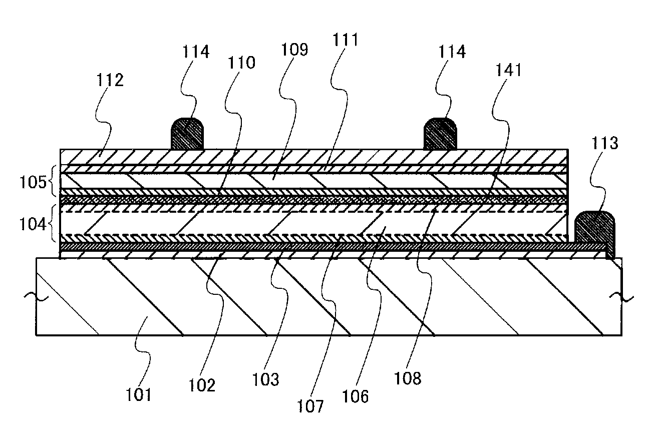
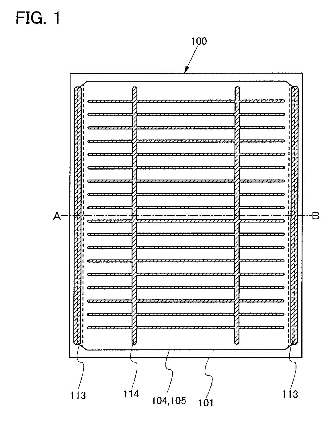
[0040]FIG. 1 is a plan view of a photoelectric conversion device 100 of this embodiment mode. This photoelectric conversion device 100 includes a first unit cell 104 and a second unit cell 105 which are fixed over a supporting substrate 101. The first unit cell 104 and the second unit cell 105 include a semiconductor junction by which photoelectric conversion is performed.

[0041]The first unit cell 104 is provided with a first electrode on the supporting substrate 101 side, and the second unit cell 105 is provided with a second electrode on the surface side. The first electrode is connected to a first auxiliary electrode 113, and a second auxiliary electrode 114 is provided over the second electrode. The photoelectric conversion device 100 of this embodiment mode has a structure in which the first unit cell 104 and the second unit cell 105 are stacked over the supporting substrate 101 having an insulating surface; therefore, positive and negative electrodes are exposed on the same su...

embodiment mode 2

[0070]In this embodiment mode, an intermediate layer which has a different structure from the intermediate layer described in Embodiment Mode 1 will be described.

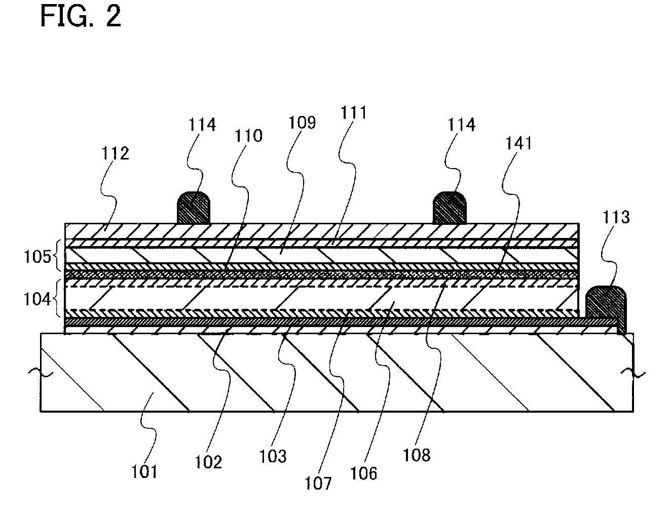
[0071]A composite material including a transition metal oxide and an organic compound can be used as the intermediate layer 141 in FIG. 2. In this specification, “composite” refers to not only a state in which two types of materials are simply mixed, but also a state in which electric charges are given and received between materials by the mixture of a plurality of materials.

[0072]Since the composite material including the transition metal oxide and the organic compound has a large carrier density, the composite material can be preferably used as a recombination center. In FIG. 5, an energy band diagram in the case where the composite material of the transition metal oxide and an organic compound is used as the intermediate layer 141 is illustrated. In the intermediate layer 141 described in this embodiment mode, electrons ...


PUM


Abstract

A photoelectric conversion device includes a first unit cell in which one face of a single crystal semiconductor layer is provided with a first electrode and a first impurity semiconductor layer including one conductivity type and an opposite face is provided with a second impurity semiconductor layer including a conductivity type opposite to the one conductivity type, and a second unit cell including a p-type organic semiconductor and an n-type organic semiconductor. The first unit cell and the second unit cell are connected in series with an intermediate layer interposed therebetween. The intermediate layer includes a transition metal oxide. A face of the first electrode which is opposite to the single crystal semiconductor layer is provided with an insulating layer, and the insulating layer is bonded to a supporting substrate.

Description

BACKGROUND OF THE INVENTION[0001]1. Field of the Invention[0002]The present invention relates to a photoelectric conversion device using a single crystal semiconductor or a polycrystalline semiconductor, and to a so-called tandem photoelectric conversion device in which a plurality of photoelectric conversion elements is stacked.[0003]2. Description of the Related Art[0004]As a measure against global warming, solar photovoltaic power generation has been spreading around the world. For the solar photovoltaic power generation, a photoelectric conversion device (also called a photovoltaic device or a solar cell) in which light energy is converted into electrical energy by using photoelectric characteristics of a semiconductor is applied in many cases, as compared to the case of using solar heat.[0005]Production of photoelectric conversion devices increases year after year. For example, the world's total production of solar cells in 2005 was increased by 47% from the previous fiscal yea...

Claims


Application Information

Patent Timeline
IPC IPC(8): H01L31/18H01L31/036H01L31/0224H01L31/06H01L31/068H01L51/42H01L51/44
CPCH01L21/76254H01L31/028H01L31/03921H01L31/0687Y02E10/547H01L51/42Y02E10/544Y02E10/549H01L31/1804Y02P70/50H10K30/00H10K30/10H01L31/022425H01L2031/0344Y02E10/50
Inventor YAMAZAKI, SHUNPEIIKEDA, HISAOSEO, SATOSHI
Owner SEMICON ENERGY LAB CO LTD
Why Eureka
Try Eureka