Nitride Semiconductor Light Emitting Device and Fabrication Method Thereof

a technology of nitride semiconductor and light emitting device, which is applied in the manufacture of semiconductor/solid-state devices, semiconductor devices, electrical devices, etc., can solve the problems of limited second electrode material formed on the second electrode contact layer, shorten the life of the light emitting device, and many problems, so as to enhance the optical power of the p-gan layer constituting the nitride semiconductor light emitting device, improve the optical power down phenomenon, and enhance the optical power

Active Publication Date: 2009-07-02
SUZHOU LEKIN SEMICON CO LTD
View PDF2 Cites 25 Cited by
  • Summary
  • Abstract
  • Description
  • Claims
  • Application Information

AI Technical Summary

Benefits of technology

[0020]According to the present invention, the characteristic of the p-GaN layer constituting the nitride semiconductor light emitting device is enhanced, the optical power of th

Problems solved by technology

Also, a second electrode material formed on the second electrode contact layer is limited depending on a doping type of the second electrode contact layer.
Meanwhile, the Mg atomic concentration remaining in the p-GaN layer 109 without a complete activation causes many problems.
For example, light emitting from the active layer toward the surface is trapped to lower the optical power, or when a high current is applied, heat is generated due to a relatively high resistance value, so that the life time of the light emitting device is shortened to have a fatal influence on the reliability.
Especially, in the

Method used


Image

  • Nitride Semiconductor Light Emitting Device and Fabrication Method Thereof
  • Nitride Semiconductor Light Emitting Device and Fabrication Method Thereof
  • Nitride Semiconductor Light Emitting Device and Fabrication Method Thereof

Examples


first embodiment

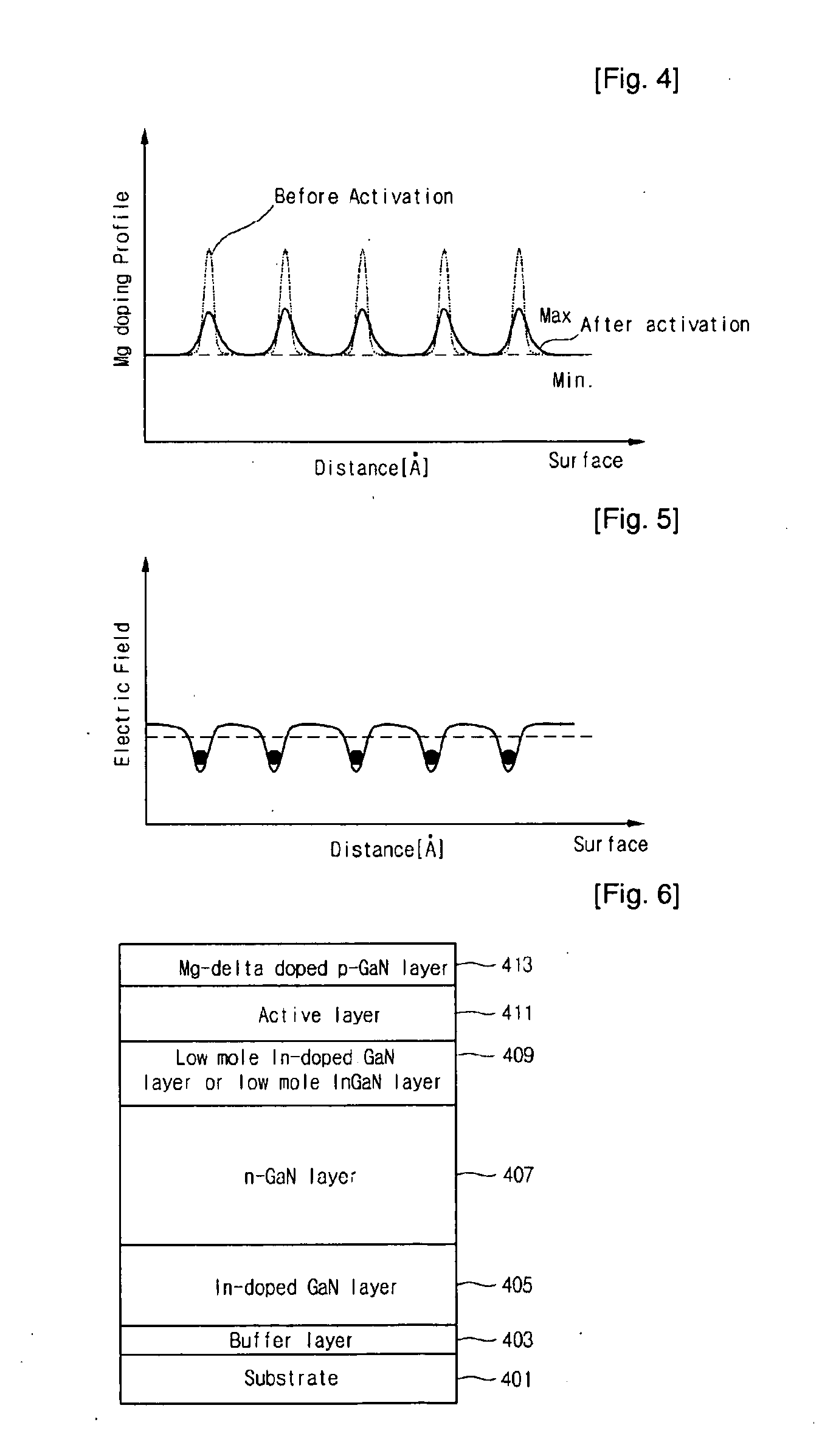
[0042]FIG. 6 is a schematic view showing a stack structure of a nitride semiconductor light emitting device according to the present invention.

[0043]Referring to FIG. 6, the nitride semiconductor light emitting device according to the present embodiment includes a substrate 401, a buffer layer 403, an In-doped GaN layer 405, an n-GaN layer 407, a low-mole In-doped GaN layer or low-mole InGaN layer 409, an active layer 411, and an Mg-delta doped p-GaN layer 413. The Mg-delta doped p-GaN layer 413 has been described in detail with reference to FIGS. 3 to 5.

[0044]Hereinafter, a fabrication method of the nitride semiconductor light emitting device according to a first embodiment will be described in more detail.

[0045]First, in the present embodiment, only H2 carrier gas is supplied onto the sapphire substrate 401 at a high temperature to clean the sapphire substrate 401. Thereafter, in step of decreasing the growth temperature to 540° C., NH3 source gas is supplied to perform a nitridat...

second embodiment

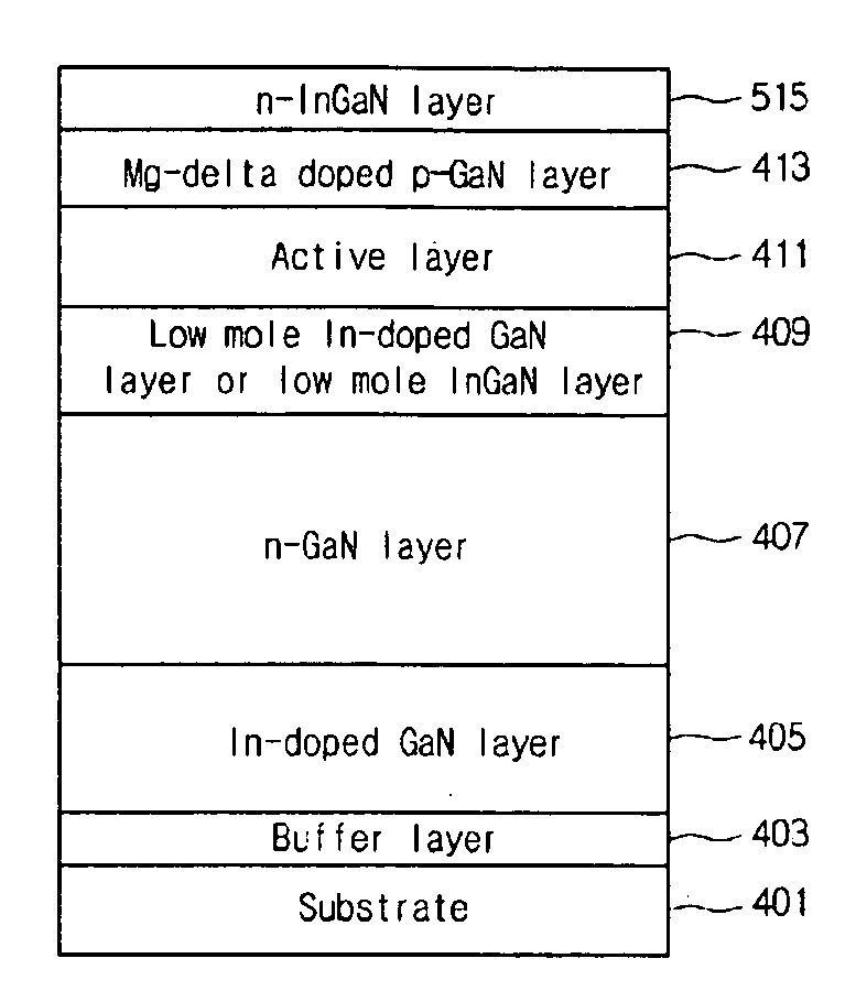
[0053]FIG. 7 shows a nitride semiconductor light emitting device according to the present invention.

[0054]Referring to FIG. 7, the nitride semiconductor light emitting device according to a second embodiment of the present invention includes a substrate 401, a buffer layer 403, an In-doped GaN layer 405, an n-GaN layer 407, a low-mole In-doped GaN layer or low-mole InGaN layer 409, an active layer 411, an Mg-delta doped p-GaN layer 413, and an n-InGaN layer 515.

[0055]Compared with the first embodiment, the above second embodiment has a difference in that the nitride semiconductor light emitting device further includes the n-InGaN layer 515. Therefore, only the n-InGaN layer 515 will be additively described and descriptions of other elements will be referred from that of the first embodiment.

[0056]To fabricate an n- / p- / n-junction structure light emitting device, in addition to the p- / n-junction structure light emitting device, the second embodiment of the present invention grows the ...


PUM


Abstract

Provided is a nitride semiconductor light emitting device including: a first nitride semiconductor layer; an active layer formed above the first nitride semiconductor layer; and a delta doped second nitride semiconductor layer formed above the active layer. According to the present invention, the optical power of the nitride semiconductor light emitting device is enhanced, optical power down phenomenon is improved and reliability against ESD (electro static discharge) is enhanced.

Description

TECHNICAL FIELD[0001]The present invention is relative to a nitride semiconductor light emitting device and fabrication method thereof, and to a nitride semiconductor light emitting device and a fabrication method thereof that can increase the optical power and enhance the reliability by increasing a hole carrier concentration contributing to the electric conductivity in an electrode contact layer to increase the recombination probability of electrons and holes.BACKGROUND ART[0002]A schematic stack structure of a general nitride semiconductor light emitting device and a fabrication method thereof will now be described.[0003]FIG. 1 is a sectional view of a general nitride semiconductor light emitting device.[0004]Referring to FIG. 1, a conventional nitride semiconductor light emitting device includes a substrate 101, a buffer layer 103, an n-GaN layer 105, an active layer 107 and a p-GaN layer 109. Herein, the substrate 101 can be exemplified by a sapphire substrate.[0005]A fabricati...

Claims


Application Information

Patent Timeline
IPC IPC(8): H01L33/00H01L33/06H01L33/12H01L33/32
CPCH01L27/15H01L33/02H01L33/06H01L33/32H01L33/025H01L33/14H01L33/305
Inventor LEE, SUK HUN
Owner SUZHOU LEKIN SEMICON CO LTD
Why Eureka
Try Eureka