Image Sensor and Manufacturing Method Thereof

a technology of image sensor and manufacturing method, which is applied in the direction of electrical apparatus, semiconductor devices, radio frequency controlled devices, etc., can solve problems such as noise or image lag, and achieve the effect of improving electron transmission efficiency

Inactive Publication Date: 2009-07-02
DONGBU HITEK CO LTD
View PDF3 Cites 27 Cited by
  • Summary
  • Abstract
  • Description
  • Claims
  • Application Information

AI Technical Summary

Benefits of technology

[0009]Embodiments of the present invention provide an image sensor and manufacturing method thereof. The image sensor can exhibit improved electron transmission efficiency by adjusting doping concentration of a channel area.

Problems solved by technology

If charges flow back toward the photodiode, noise or image lag may occur.

Method used


Image

  • Image Sensor and Manufacturing Method Thereof
  • Image Sensor and Manufacturing Method Thereof
  • Image Sensor and Manufacturing Method Thereof

Examples


Embodiment Construction

[0014]When the terms “on” or “over” or “above” are used herein, when referring to layers, regions, patterns, or structures, it is understood that the layer, region, pattern, or structure can be directly on another layer or structure, or intervening layers, regions, patterns, or structures may also be present. When the terms “under” or “below” are used herein, when referring to layers, regions, patterns, or structures, it is understood that the layer, region, pattern, or structure can be directly under the other layer or structure, or intervening layers, regions, patterns, or structures may also be present.

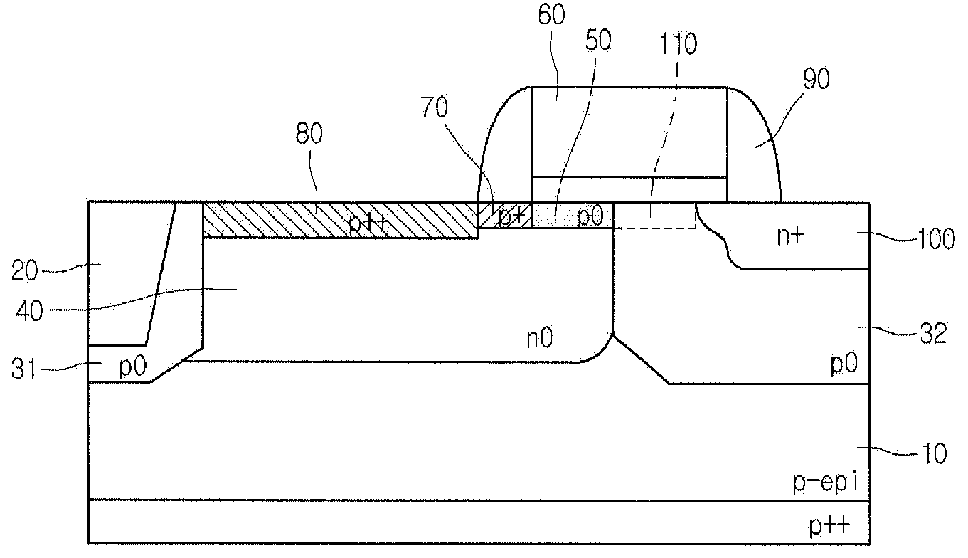
[0015]FIG. 5 is a cross-sectional view showing an image sensor according to an embodiment of the present invention.

[0016]Referring to FIG. 5, an image sensor can include a gate 60 on a semiconductor substrate 10, a first p-type doping area 50 and a second p-type doping area 110 disposed below the gate 60, a third p-type doping area 70, a fourth p-type doping area 80, an n-type dopi...


PUM


Abstract

An image sensor and manufacturing method thereof are provided. The image sensor can include a gate on a semiconductor substrate, first and second p-type doping areas below the gate, a third p-type doping area adjacent to the first p-type doping area, and a fourth p-type doping area adjacent to the third p-type doping area. An n-type doping area can be provided in the semiconductor substrate such that at least a portion of the n-type doping area is disposed below the first, third, and fourth p-type doping areas. A floating diffusion area can be provided adjacent to the second p-type doping area.

Description

CROSS-REFERENCE TO RELATED APPLICATION[0001]The present application claims the benefit under 35 U.S.C. § 119 of Korean Patent Application No. 10-2007-0138549, filed Dec. 27, 2007, which is hereby incorporated by reference in its entirety.BACKGROUND[0002]An image sensor is a semiconductor device for converting an optical image into an electric signal. An image sensor can be categorized as a charge coupled device (CCD) image sensor or a complementary metal oxide semiconductor (CMOS) image sensor.[0003]A CMOS image sensor typically employs a switching mode to sequentially detect output by providing metal oxide semiconductor (MOS) transistors corresponding to the number of pixels through CMOS technology, and using peripheral devices, such as control circuits and signal processing circuits.[0004]Also, a CMOS image sensor generally includes a photodiode for receiving light to generate photocharges and a MOS transistor arranged according to unit pixels.[0005]A MOS transistor circuit for a ...

Claims


Application Information

Patent Timeline
Patent Type & Authority Applications(United States)
IPC IPC(8): H01L27/146H01L31/18
CPCH01L27/14689H01L27/14603H01L27/146
Inventor KIM, JONG MIN
Owner DONGBU HITEK CO LTD
Why Eureka
Try Eureka